Understanding PCB Wiring Basics
Before diving into the wiring process, it’s crucial to understand the basics of PCB wiring. This section will cover the essential components and concepts you’ll encounter when working with PCBs.
Components of a PCB
A PCB consists of several key components:
- Substrate: The base material, usually made of fiberglass or other insulating materials.
- Copper layers: Thin sheets of copper laminated onto the substrate, forming the conductive pathways.
- Solder mask: A protective layer that covers the copper traces, leaving only the exposed pads for soldering.
- Silkscreen: Text and symbols printed on the PCB for component identification and orientation.
Types of PCB Wiring
There are two primary types of PCB wiring:
- Through-hole wiring: Components with long leads are inserted through drilled holes in the PCB and soldered on the opposite side.
- Surface-mount wiring: Components are soldered directly onto the surface of the PCB, requiring no drilled holes.
Tools and Materials Required for PCB Wiring
To perform PCB wiring efficiently, you’ll need the following tools and materials:
- Soldering iron
- Solder wire (lead-free recommended)
- Soldering iron tip cleaner
- Solder wick or desoldering pump
- Wire cutters
- Wire strippers
- Tweezers
- Magnifying glass or microscope
- Flux (optional)
Step-by-Step Guide to PCB Wiring
Now that you have a basic understanding of PCB wiring and the necessary tools, let’s walk through the step-by-step process of wiring a PCB.
Step 1: Prepare the PCB
- Clean the PCB surface with isopropyl alcohol to remove any dirt or grease.
- Inspect the PCB for any defects or damaged components.
- Place the PCB in a stable, well-lit workspace.
Step 2: Install Through-Hole Components
- Insert the leads of through-hole components into their designated holes on the PCB.
- Bend the leads slightly outward on the opposite side to hold the components in place.
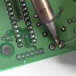
- Solder the leads to the PCB pads, ensuring a secure connection.
- Trim any excess lead wire with wire cutters.
Step 3: Install Surface-Mount Components
- Apply a small amount of solder paste or flux to the PCB pads for surface-mount components.
- Place the surface-mount components onto their designated pads using tweezers.
- Carefully solder the components to the pads, ensuring proper alignment and connection.
Step 4: Inspect and Clean the Wiring
- Visually inspect the soldered connections for any bridging, cold joints, or incomplete connections.
- Use a magnifying glass or microscope for a more detailed inspection.
- Clean any excess flux residue with isopropyl alcohol and a soft brush.
Step 5: Test the PCB
- Connect the PCB to a power source and test its functionality.
- Use a multimeter to check for continuity and proper voltage levels.
- Make any necessary adjustments or repairs based on the test results.

Common PCB Wiring Techniques
In this section, we’ll explore some common PCB wiring techniques that can help you achieve better results and overcome specific challenges.
Proper Soldering Technique
Mastering the art of soldering is essential for successful PCB wiring. Follow these tips for proper soldering:
- Keep the soldering iron tip clean and well-tinned.
- Set the soldering iron temperature appropriate for the solder type and component size.
- Apply heat to both the PCB pad and the component lead simultaneously.
- Feed solder into the joint, allowing it to flow evenly around the connection.
- Remove the soldering iron and let the joint cool without disturbing it.
Dealing with Tight Spaces
Wiring PCBs with high component density can be challenging. Use these techniques to manage tight spaces:
- Use tweezers or fine-tipped pliers to position components accurately.
- Apply flux to improve solder flow and reduce the risk of bridging.
- Use a smaller soldering iron tip for precise control in tight areas.
- Consider using a hot air soldering station for surface-mount components in congested areas.
Avoiding Common Wiring Mistakes
To ensure a reliable and functional PCB, avoid these common wiring mistakes:
- Cold joints: Caused by insufficient heat or improper solder flow. Reheat and apply more solder if necessary.
- Bridging: Accidentally connecting adjacent pads or traces with solder. Use solder wick or a desoldering pump to remove excess solder.
- Overheating: Applying too much heat can damage components or lift pads. Use the lowest effective temperature and minimize heat exposure.
- Incorrect component orientation: Double-check component placement and orientation before soldering.
Advanced PCB Wiring Techniques
For more advanced PCB wiring projects, consider these techniques:
Using a Soldering Station
A soldering station offers more precise temperature control and additional features compared to a basic soldering iron. Benefits include:
- Adjustable temperature settings for different Solder Types and components.
- Interchangeable tips for various wiring tasks.
- Built-in standby mode and automatic shut-off for safety.
Employing a Reflow Oven
A reflow oven is used for soldering surface-mount components on a PCB. The process involves:
- Applying solder paste to the PCB pads.
- Placing components onto the solder paste.
- Heating the PCB in the reflow oven to melt the solder and create secure connections.
Utilizing a Solder Stencil
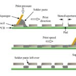
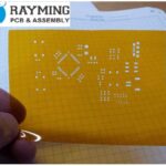
A solder stencil is a thin metal sheet with apertures that match the PCB pad layout. It is used to apply solder paste evenly and accurately. To use a solder stencil:
- Align the stencil with the PCB.
- Apply solder paste over the stencil, using a squeegee to spread it evenly.
- Carefully remove the stencil, leaving precise amounts of solder paste on the pads.
Troubleshooting PCB Wiring Issues
Despite following best practices, you may encounter issues during PCB wiring. This section covers common problems and their solutions.
Continuity Issues
If your PCB fails to function properly, check for continuity issues:
- Use a multimeter to test for continuity between connected points.
- Check for broken traces, damaged components, or poor solder joints.
- Repair or replace faulty components and resolder any suspect connections.
Signal Interference
Signal interference can cause PCB malfunction. To minimize interference:
- Ensure proper grounding and shielding of sensitive components.
- Separate high-frequency and low-frequency signals.
- Use Decoupling capacitors to reduce power supply noise.
- Consider using a ground plane to provide a low-impedance return path for signals.
Overheating Components
Overheating can damage components and cause PCB failure. To prevent overheating:
- Ensure proper heat dissipation through adequate PCB design and component placement.
- Use heatsinks or thermal management techniques for high-power components.
- Monitor component temperatures during operation and adjust cooling if necessary.
FAQ
-
What is the difference between through-hole and surface-mount wiring?
Through-hole wiring involves inserting component leads through drilled holes in the PCB and soldering them on the opposite side. Surface-mount wiring involves soldering components directly onto the surface of the PCB without using drilled holes. -
Can I mix through-hole and surface-mount components on the same PCB?
Yes, it is possible to use both through-hole and surface-mount components on the same PCB. This is known as a mixed-technology PCB. However, it’s essential to consider the design and manufacturing implications of mixing the two technologies. -
What type of solder should I use for PCB wiring?
Lead-free solder is recommended for PCB wiring due to environmental and health concerns. Common lead-free solder alloys include tin-silver-copper (SAC) and tin-copper (SnCu). Choose a solder wire with a diameter appropriate for your soldering iron tip and the size of the components being soldered. -
How do I prevent bridging when soldering closely spaced components?
To prevent bridging, use a fine-tipped soldering iron and apply solder sparingly. Additionally, using flux can help the solder flow more easily and reduce the risk of bridging. If bridging does occur, use solder wick or a desoldering pump to remove the excess solder. -
What should I do if I accidentally lift a PCB pad during soldering?
If a PCB pad is lifted during soldering, you can attempt to repair it using the following steps: - Clean the affected area with isopropyl alcohol.
- Apply a small amount of solder to the lifted pad and the exposed trace.
- Use a fine wire or a small piece of copper tape to bridge the connection between the pad and the trace.
- Solder the wire or tape in place, ensuring a secure connection.
If the damage is extensive or the repair is unsuccessful, consider using a wire jumper to connect the component to an alternative pad or trace.
Conclusion
PCB wiring is a crucial skill for anyone working with electronic circuits. By understanding the basics, using the right tools and techniques, and following best practices, you can create reliable and well-functioning PCBs. Remember to take your time, practice proper soldering techniques, and pay attention to detail. With experience and patience, you’ll be able to tackle increasingly complex PCB wiring projects with confidence.
Leave a Reply