Insufficient Wetting
Insufficient wetting occurs when the solder does not flow properly onto the surface of the PCB or the component leads. This can result in a weak or incomplete solder joint, which can lead to electrical failures.
Causes of Insufficient Wetting
- Contaminated or oxidized surfaces
- Incorrect solder temperature
- Insufficient flux
- Incorrect solder alloy
Solutions to Insufficient Wetting
- Clean and prepare surfaces properly before soldering
- Use the correct solder temperature for the specific application
- Apply sufficient flux to the joint
- Use the correct solder alloy for the specific application
Bridging
Bridging occurs when solder inadvertently connects two or more adjacent pads or traces on the PCB. This can cause short circuits and other electrical issues.
Causes of Bridging
- Excessive solder
- Incorrect solder temperature
- Incorrect soldering technique
- Incorrect component placement
Solutions to Bridging
- Use the correct amount of solder for the specific application
- Use the correct solder temperature for the specific application
- Use proper soldering techniques, such as avoiding excessive solder and maintaining a steady hand
- Ensure components are placed correctly on the PCB
Cold Joints
Cold joints occur when the solder does not melt completely, resulting in a dull, grainy appearance. Cold joints are weak and can lead to electrical failures.
Causes of Cold Joints
- Incorrect solder temperature
- Insufficient heat transfer
- Contaminated surfaces
- Incorrect soldering technique
Solutions to Cold Joints
- Use the correct solder temperature for the specific application
- Ensure sufficient heat transfer by using a properly sized soldering iron tip and applying heat to both the component lead and the PCB pad
- Clean and prepare surfaces properly before soldering
- Use proper soldering techniques, such as maintaining a steady hand and applying solder quickly and efficiently

Tombstoning
Tombstoning occurs when a surface-mount component stands up on one end during the soldering process. This can cause the component to disconnect from the PCB and lead to electrical failures.
Causes of Tombstoning
- Uneven heating of the component
- Incorrect component placement
- Incorrect solder paste application
- Incorrect reflow profile
Solutions to Tombstoning
- Ensure even heating of the component by using a properly sized soldering iron tip and applying heat to both the component leads and the PCB pads
- Ensure components are placed correctly on the PCB
- Apply solder paste evenly and in the correct amount
- Use the correct reflow profile for the specific application
Solder Balls
Solder balls are small, spherical balls of solder that can form on the surface of the PCB during the soldering process. They can cause short circuits and other electrical issues.
Causes of Solder Balls
- Excessive solder
- Incorrect solder temperature
- Incorrect soldering technique
- Contaminated surfaces
Solutions to Solder Balls
- Use the correct amount of solder for the specific application
- Use the correct solder temperature for the specific application
- Use proper soldering techniques, such as avoiding excessive solder and maintaining a steady hand
- Clean and prepare surfaces properly before soldering
Solder Bridges
Solder bridges are similar to bridging, but they occur when solder flows between two adjacent pads or traces on the PCB, creating an unintended connection.
Causes of Solder Bridges
- Excessive solder
- Incorrect solder temperature
- Incorrect soldering technique
- Incorrect component placement
Solutions to Solder Bridges
- Use the correct amount of solder for the specific application
- Use the correct solder temperature for the specific application
- Use proper soldering techniques, such as avoiding excessive solder and maintaining a steady hand
- Ensure components are placed correctly on the PCB
Lifted Pads
Lifted pads occur when the copper pad on the PCB separates from the board during the soldering process. This can cause the component to disconnect from the PCB and lead to electrical failures.
Causes of Lifted Pads
- Excessive heat
- Incorrect soldering technique
- Poor PCB design or manufacturing
- Contaminated surfaces
Solutions to Lifted Pads
- Use the correct solder temperature for the specific application
- Use proper soldering techniques, such as avoiding excessive heat and maintaining a steady hand
- Ensure PCBs are designed and manufactured to high standards
- Clean and prepare surfaces properly before soldering
Flux Residue
Flux residue is a byproduct of the soldering process that can accumulate on the surface of the PCB. It can cause corrosion and other issues if not properly cleaned.
Causes of Flux Residue
- Insufficient cleaning after soldering
- Incorrect flux type
- Excessive flux application
Solutions to Flux Residue
- Clean PCBs thoroughly after soldering using appropriate cleaning agents and techniques
- Use the correct flux type for the specific application
- Apply flux in the correct amount and only where necessary
Solder Whiskers
Solder whiskers are thin, hairlike protrusions that can grow from solder joints over time. They can cause short circuits and other electrical issues.
Causes of Solder Whiskers
- Use of lead-free solder
- Incorrect storage conditions
- Mechanical stress on solder joints
Solutions to Solder Whiskers
- Use solder alloys that are less prone to whisker growth, such as those containing lead
- Store PCBs in a cool, dry environment with minimal temperature fluctuations
- Minimize mechanical stress on solder joints through proper design and handling
Incorrect Component Orientation
Incorrect component orientation occurs when a component is placed on the PCB in the wrong direction or orientation. This can cause the component to malfunction or not function at all.
Causes of Incorrect Component Orientation
- Human error during manual assembly
- Incorrect component packaging or labeling
- Incorrect PCB design or silkscreen markings
Solutions to Incorrect Component Orientation
- Use automated assembly processes when possible to minimize human error
- Verify component packaging and labeling before assembly
- Ensure PCB designs and silkscreen markings are clear and accurate
Poor Hole Filling
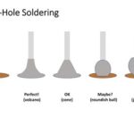
Poor hole filling occurs when solder does not completely fill the holes in through-hole components, resulting in a weak or incomplete solder joint.
Causes of Poor Hole Filling
- Insufficient solder
- Incorrect soldering technique
- Contaminated or oxidized surfaces
- Incorrect hole size or shape
Solutions to Poor Hole Filling
- Use the correct amount of solder for the specific application
- Use proper soldering techniques, such as applying heat to both the component lead and the PCB pad and allowing sufficient time for the solder to flow
- Clean and prepare surfaces properly before soldering
- Ensure hole sizes and shapes are appropriate for the specific component
Solder mask damage
Solder mask damage occurs when the solder mask, a protective coating on the PCB, is damaged during the soldering process. This can expose the underlying copper and lead to corrosion and other issues.
Causes of Solder Mask Damage
- Excessive heat
- Incorrect soldering technique
- Poor solder mask quality or application
- Mechanical damage during handling
Solutions to Solder Mask Damage
- Use the correct solder temperature for the specific application
- Use proper soldering techniques, such as avoiding excessive heat and maintaining a steady hand
- Ensure solder mask is of high quality and applied correctly during PCB manufacturing
- Handle PCBs carefully to avoid mechanical damage
Insufficient Clearance
Insufficient clearance occurs when components are placed too close together on the PCB, making it difficult to solder them properly and increasing the risk of solder bridges and other issues.
Causes of Insufficient Clearance
- Poor PCB design
- Incorrect component placement
- Use of oversized components
Solutions to Insufficient Clearance
- Ensure PCB designs provide sufficient clearance between components
- Use automated assembly processes when possible to ensure accurate component placement
- Select components that are appropriately sized for the specific application
Solder Joint Fractures
Solder joint fractures occur when the solder joint cracks or breaks due to mechanical stress or thermal cycling. This can cause the component to disconnect from the PCB and lead to electrical failures.
Causes of Solder Joint Fractures
- Insufficient solder
- Poor solder joint geometry
- Mechanical stress or vibration
- Thermal cycling
Solutions to Solder Joint Fractures
- Use the correct amount of solder for the specific application
- Ensure solder joint geometry is appropriate for the specific application
- Use underfill or other reinforcement techniques to minimize mechanical stress on solder joints
- Design PCBs and select components to minimize thermal stress on solder joints
Incompatible Materials
Incompatible materials occur when the solder, flux, or other materials used in the soldering process are not compatible with each other or with the PCB or components. This can cause poor solder joint quality, corrosion, and other issues.
Causes of Incompatible Materials
- Use of incorrect solder alloy or flux
- Contamination of solder or flux
- Incorrect PCB or component materials
Solutions to Incompatible Materials
- Select solder alloys and fluxes that are compatible with each other and with the specific application
- Store solder and flux properly to avoid contamination
- Ensure PCBs and components are made from compatible materials
Frequently Asked Questions (FAQ)
1. What is the most common PCB Soldering problem?
The most common PCB soldering problem is insufficient wetting, which occurs when the solder does not flow properly onto the surface of the PCB or the component leads. This can result in a weak or incomplete solder joint, which can lead to electrical failures.
2. How can I prevent solder bridges?
To prevent solder bridges, use the correct amount of solder for the specific application, use the correct solder temperature, use proper soldering techniques such as avoiding excessive solder and maintaining a steady hand, and ensure components are placed correctly on the PCB.
3. What causes tombstoning?
Tombstoning occurs when a surface-mount component stands up on one end during the soldering process. This can be caused by uneven heating of the component, incorrect component placement, incorrect solder paste application, or an incorrect reflow profile.
4. How can I remove flux residue from my PCB?
To remove flux residue from your PCB, clean the board thoroughly after soldering using appropriate cleaning agents and techniques. Isopropyl alcohol is a common cleaning agent used for this purpose.
5. Can solder whiskers cause permanent damage to my PCB?
Yes, solder whiskers can cause permanent damage to your PCB if they cause a short circuit or other electrical issue. To minimize the risk of solder whiskers, use solder alloys that are less prone to whisker growth, store PCBs in a cool, dry environment with minimal temperature fluctuations, and minimize mechanical stress on solder joints through proper design and handling.
| Problem | Causes | Solutions |
|---|---|---|
| Insufficient Wetting | Contaminated surfaces, incorrect temperature, insufficient flux | Clean surfaces, use correct temperature and flux |
| Bridging | Excessive solder, incorrect temperature, incorrect technique | Use correct amount of solder, temperature, and technique; ensure proper component placement |
| Cold Joints | Incorrect temperature, insufficient heat transfer, contamination | Use correct temperature, ensure heat transfer, clean surfaces, use proper technique |
| Tombstoning | Uneven heating, incorrect placement, paste application, or reflow | Ensure even heating, correct placement, paste application, and reflow profile |
| Solder Balls | Excessive solder, incorrect temperature, technique, contamination | Use correct amount of solder, temperature, and technique; clean surfaces |
| Solder Bridges | Excessive solder, incorrect temperature, technique, placement | Use correct amount of solder, temperature, and technique; ensure proper component placement |
| Lifted Pads | Excessive heat, incorrect technique, poor design, contamination | Use correct temperature, proper technique, ensure PCB quality, clean surfaces |
| Flux Residue | Insufficient cleaning, incorrect flux type or amount | Clean thoroughly, use correct flux type and amount |
| Solder Whiskers | Lead-free solder, incorrect storage, mechanical stress | Use lead solder, store properly, minimize stress |
| Incorrect Orientation | Human error, incorrect packaging or design | Use automation, verify packaging and design |
| Poor Hole Filling | Insufficient solder, incorrect technique, contamination, hole size | Use correct amount of solder and technique, clean surfaces, ensure proper hole size |
| Solder Mask Damage | Excessive heat, incorrect technique, poor quality, mechanical damage | Use correct temperature and technique, ensure mask quality, handle carefully |
| Insufficient Clearance | Poor design, incorrect placement, oversized components | Ensure proper design and placement, select appropriate components |
| Solder Joint Fractures | Insufficient solder, poor geometry, mechanical stress, thermal cycling | Use correct amount of solder, ensure proper geometry, minimize stress, design for thermal cycles |
| Incompatible Materials | Incorrect solder or flux, contamination, incorrect PCB or components | Select compatible materials, store properly, ensure PCB and component compatibility |
By understanding these common PCB Soldering Problems and their causes and solutions, you can improve your soldering skills and ensure the reliability and functionality of your electronic devices. Remember to always use proper techniques, materials, and equipment, and to stay up-to-date with best practices and industry standards. With practice and attention to detail, you can achieve high-quality solder joints and avoid these common pitfalls.
Leave a Reply