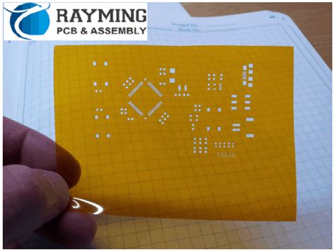
What is a Solder Stencil?
A solder stencil is a thin, flat sheet of material with precisely cut apertures that correspond to the pads on a PCB where solder paste needs to be applied. The stencil is placed over the PCB, and solder paste is spread across the surface using a squeegee or automated dispensing equipment. The solder paste is deposited onto the pads through the apertures, ensuring a precise and uniform amount of paste is applied to each pad.
Types of Solder Stencils
There are several types of solder stencils available, each with its own advantages and disadvantages. The most common types include:
-
Laser-cut stencils: These stencils are cut using a high-precision laser, resulting in clean, burr-free apertures with tight tolerances. Laser-cut stencils are suitable for most PCB designs and offer excellent paste release characteristics.
-
Chemical-etched stencils: Chemical-etched stencils are created by exposing a photosensitive material to a pattern and then chemically etching away the unwanted areas. This process is less precise than laser cutting but can be more cost-effective for larger apertures and simpler designs.
-
Electroformed stencils: Electroformed stencils are created by electroplating nickel onto a master pattern, resulting in a thin, durable stencil with smooth aperture walls. These stencils are ideal for fine-pitch applications and offer excellent paste release characteristics.
Solder Stencil Materials
Solder stencils can be made from various materials, each with its own properties and benefits. The most common materials include:
-
Stainless steel: Stainless steel is the most widely used material for solder stencils due to its durability, stability, and excellent paste release characteristics. It is available in various thicknesses and grades to suit different applications.
-
Nickel: Nickel stencils, particularly electroformed nickel, are known for their excellent dimensional stability and smooth aperture walls. They are ideal for fine-pitch applications and offer superior paste release compared to stainless steel.
-
Polyimide: Polyimide stencils, also known as plastic stencils, are lightweight, flexible, and cost-effective. They are suitable for low-volume production or prototyping but may not offer the same durability and precision as metal stencils.
Solder Stencil Design Considerations
Designing a solder stencil involves several key considerations to ensure optimal solder paste application and PCB assembly quality. These include:
Aperture Size and Shape
The size and shape of the apertures in a solder stencil directly impact the amount of solder paste deposited onto the pads. Aperture size is typically expressed as a percentage of the pad size, with common area ratios ranging from 80% to 100%. The optimal aperture size depends on factors such as pad size, pitch, and solder paste properties.
Aperture shape also plays a role in paste release and print quality. Common aperture shapes include square, circular, and home plate (rounded rectangle). The choice of aperture shape depends on the pad geometry and the specific requirements of the PCB design.
Stencil Thickness
Stencil thickness is another critical factor in determining the volume of solder paste deposited onto the pads. Thicker stencils deposit more paste, while thinner stencils deposit less. The optimal stencil thickness depends on the component pitch, pad size, and solder paste properties. Common stencil thicknesses range from 0.100mm to 0.150mm (4 to 6 mils) for standard SMT applications, and 0.050mm to 0.100mm (2 to 4 mils) for fine-pitch applications.
| Pitch | Recommended Stencil Thickness |
|---|---|
| ≥ 0.65mm | 0.100mm – 0.150mm (4-6 mils) |
| 0.5 – 0.65mm | 0.075mm – 0.100mm (3-4 mils) |
| 0.4 – 0.5mm | 0.050mm – 0.075mm (2-3 mils) |
| < 0.4mm | 0.050mm (2 mils) or less |
Aperture Wall Angle
The angle of the aperture walls in a solder stencil can affect paste release and print quality. Most stencils have aperture walls that are slightly tapered, typically between 5° and 15°, to facilitate paste release. A higher wall angle can improve paste release but may also increase the risk of bridging between adjacent pads. The optimal wall angle depends on the aperture size, pitch, and solder paste properties.
Fiducial Marks and Tooling Holes
Fiducial marks and tooling holes are essential features in a solder stencil that aid in alignment and registration during the printing process. Fiducial marks are small, precisely placed features that serve as reference points for aligning the stencil with the PCB. They are typically located at the corners or edges of the stencil and should be compatible with the vision systems used in the assembly equipment.
Tooling holes are larger openings in the stencil that correspond to the tooling pins on the PCB or the printing equipment. These holes help to secure the stencil in place during printing and ensure consistent alignment between the stencil and the PCB.

Solder Paste Printing Process
The solder paste printing process involves several steps to ensure consistent and accurate solder paste deposition. These steps include:
-
Stencil alignment: The solder stencil is aligned with the PCB using the fiducial marks and tooling holes. Proper alignment is critical to ensure that the solder paste is deposited accurately onto the pads.
-
Solder paste application: Solder paste is applied to the stencil surface and spread across the apertures using a squeegee or automated dispensing equipment. The squeegee pressure, speed, and angle are adjusted to achieve optimal paste deposition and release.
-
Stencil separation: After printing, the stencil is carefully separated from the PCB to avoid disturbing the deposited solder paste. The separation speed and angle are controlled to minimize the risk of paste smearing or slumping.
-
Inspection: The printed PCB is inspected for defects such as insufficient paste, bridging, or misalignment. Automated solder paste inspection (SPI) systems are often used to quickly and accurately assess the quality of the solder paste deposition.

Best Practices for Solder Stencil Usage and Maintenance
To ensure consistent and high-quality solder paste printing, it is essential to follow best practices for solder stencil usage and maintenance. These include:
-
Proper storage: Solder stencils should be stored in a clean, dry environment to prevent damage or contamination. They should be kept flat or hung vertically to avoid warping or deformation.
-
Regular cleaning: Solder stencils should be cleaned regularly to remove excess solder paste, debris, or contamination. Cleaning can be done using solvents, ultrasonic cleaners, or specialized stencil cleaning equipment. Proper cleaning helps to maintain print quality and extend the life of the stencil.
-
Inspection and repair: Solder stencils should be inspected periodically for signs of wear, damage, or clogged apertures. Minor damage or clogged apertures can often be repaired using specialized tools or techniques, such as laser welding or micro-blasting. However, severely damaged or worn stencils should be replaced to ensure consistent print quality.
-
Handling and transport: Solder stencils should be handled with care to avoid damage or contamination. When transporting stencils, they should be properly packaged and protected to prevent warping, bending, or other damage.

Frequently Asked Questions (FAQ)
-
What is the difference between a solder stencil and a solder screen?
A solder stencil is a thin, flat sheet of material with precisely cut apertures, while a solder screen is a woven mesh with a patterned emulsion. Stencils offer better print definition and are more suitable for fine-pitch applications, while screens are more flexible and can be more cost-effective for larger components or lower-volume production. -
How often should I clean my solder stencil?
The frequency of cleaning depends on factors such as the type of solder paste, the volume of production, and the environment. In general, solder stencils should be cleaned at least once per shift or every 4-8 hours of continuous use. However, more frequent cleaning may be necessary for high-volume production or when using certain types of solder paste. -
Can I reuse a damaged or worn solder stencil?
It depends on the extent of the damage or wear. Minor damage or clogged apertures can often be repaired using specialized tools or techniques. However, severely damaged or worn stencils should be replaced to ensure consistent print quality and avoid defects in the assembled PCBs. -
What is the optimal aperture size for my components?
The optimal aperture size depends on factors such as the component pitch, pad size, and solder paste properties. As a general guideline, the aperture size should be between 80% and 100% of the pad size. However, it is essential to consult with your stencil manufacturer or use stencil design software to determine the optimal aperture size for your specific application. -
How do I choose the right solder paste for my stencil printing process?
Choosing the right solder paste involves considering factors such as the alloy composition, particle size, flux type, and rheological properties. The solder paste should be compatible with the stencil aperture sizes, the component types and sizes, and the reflow profile. It is essential to consult with your solder paste supplier or conduct testing to determine the best solder paste for your specific application.
Conclusion
Solder stencils play a critical role in ensuring precise and consistent solder paste application in PCB assembly. By understanding the types, materials, design considerations, and best practices for solder stencil usage and maintenance, you can optimize your solder paste printing process and achieve high-quality, reliable PCB assemblies. Whether you are a novice or an experienced professional in PCB assembly, investing in the right solder stencil and following best practices can help you to improve your productivity, reduce defects, and enhance the overall quality of your products.


Leave a Reply