Introduction to PCB Prototypes
Printed Circuit Board (PCB) prototypes are essential for testing and validating the design of electronic circuits before mass production. PCB Prototyping allows designers to identify and fix any issues in the circuit design, component placement, and functionality. In this article, we will explore the process of manufacturing and assembling PCB prototypes, focusing on the 3+3 approach.
What is the 3+3 Approach in PCB Prototyping?
The 3+3 approach in PCB prototyping refers to the practice of manufacturing three bare PCBs and assembling three of them with components. This approach offers several advantages:
- Redundancy: Having three assembled PCBs ensures that if one fails, you have backup units for testing and debugging.
- Comparison: With three identical PCBs, you can compare their performance and identify any inconsistencies or manufacturing defects.
- Validation: Assembling three PCBs allows for thorough testing and validation of the circuit design and component compatibility.
Advantages of the 3+3 Approach
| Advantage | Description |
|---|---|
| Redundancy | Backup units for testing and debugging |
| Comparison | Identify inconsistencies or manufacturing defects |
| Validation | Thorough testing and validation of circuit design |
PCB Prototyping Process
The PCB prototyping process involves several steps, from design to manufacturing and assembly. Let’s explore each step in detail.
Step 1: PCB Design
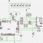
The first step in PCB prototyping is to design the circuit using Electronic Design Automation (EDA) software. The design process includes:
- Schematic capture: Creating a schematic diagram of the electronic circuit.
- Component selection: Choosing the appropriate components for the circuit based on their specifications and functionality.
- PCB layout: Designing the physical layout of the PCB, including component placement, trace routing, and layer stackup.
Step 2: Design Review and Verification
After completing the PCB design, it is crucial to review and verify the design before proceeding to manufacturing. This step involves:
- Design rule check (DRC): Verifying that the PCB layout adheres to the manufacturing and assembly guidelines.
- Electrical rule check (ERC): Ensuring that the circuit connections and component pins are properly connected and free from shorts or open circuits.
- Gerber File Generation: Creating the necessary Gerber files for PCB manufacturing, including copper layers, solder mask, silkscreen, and drill files.
Step 3: PCB Manufacturing
With the verified design files, the next step is to manufacture the bare PCBs. The manufacturing process includes:
- Material selection: Choosing the appropriate PCB substrate material, such as FR-4, based on the application requirements.
- Copper Clad lamination: Laminating the substrate with copper foil on one or both sides.
- Photoresist application: Applying a photosensitive resist layer on the copper surface.
- Exposure and development: Exposing the photoresist to UV light through a photomask and developing the exposed areas.
- Etching: Removing the unwanted copper areas using an etchant solution, leaving only the desired circuit traces.
- Drill holes and vias: Drilling the necessary holes and vias for component mounting and inter-layer connections.
- Surface finish application: Applying a surface finish, such as HASL, ENIG, or OSP, to protect the copper traces and improve solderability.
| PCB Manufacturing Step | Description |
|---|---|
| Material selection | Choose appropriate substrate material |
| Copper clad lamination | Laminate substrate with copper foil |
| Photoresist application | Apply photosensitive resist layer |
| Exposure and development | Expose photoresist to UV light and develop |
| Etching | Remove unwanted copper areas |
| Drill holes and vias | Drill necessary holes and vias |
| Surface finish application | Apply surface finish for protection and solderability |
Step 4: PCB Assembly
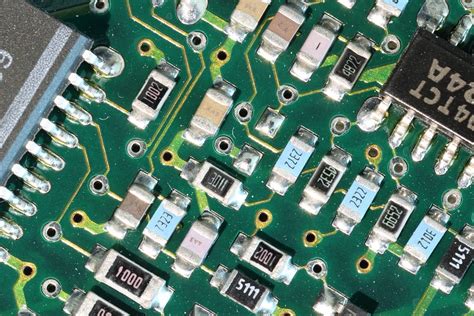
After manufacturing the bare PCBs, the next step is to assemble the components onto the PCBs. The assembly process includes:
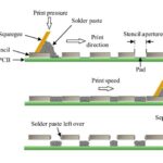
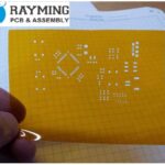
- Solder paste application: Applying solder paste onto the component pads using a stencil or syringe.
- Component placement: Placing the components onto the PCB using pick-and-place machines or manual placement.
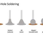
- Reflow soldering: Passing the PCB through a reflow oven to melt the solder paste and form a permanent connection between the components and the PCB.
- Inspection and testing: Visually inspecting the assembled PCBs for any defects or misaligned components and performing electrical tests to ensure proper functionality.
| PCB Assembly Step | Description |
|---|---|
| Solder paste application | Apply solder paste onto component pads |
| Component placement | Place components onto PCB |
| Reflow soldering | Pass PCB through reflow oven to form connections |
| Inspection and testing | Visually inspect and perform electrical tests |
Step 5: Debugging and Rework
Despite thorough design verification and careful assembly, issues may still arise in the assembled PCB prototypes. Debugging and rework involve:
- Identifying the issue: Using diagnostic tools and techniques to pinpoint the source of the problem, such as faulty components, incorrect connections, or design flaws.
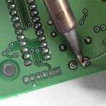
- Rework: Removing and replacing faulty components, fixing incorrect connections, or making necessary design modifications.
- Retesting: Verifying that the reworked PCB prototypes function as intended and meet the design specifications.

Benefits of Professional PCB Prototyping Services
While it is possible to manufacture and assemble PCB prototypes in-house, using professional PCB prototyping services offers several benefits:
- Expertise: Professional PCB manufacturers have the expertise and experience to handle complex PCB designs and ensure high-quality results.
- Advanced equipment: PCB prototyping services have access to advanced manufacturing and assembly equipment, ensuring precise and reliable results.
- Time and cost savings: Outsourcing PCB prototyping allows designers to focus on other aspects of product development, saving time and reducing overall costs.
- Scalability: Professional PCB prototyping services can easily scale up production when transitioning from prototypes to mass production.
| Benefit | Description |
|---|---|
| Expertise | Experienced professionals ensure high-quality results |
| Advanced equipment | Access to advanced manufacturing and assembly equipment |
| Time and cost savings | Outsourcing allows designers to focus on other aspects |
| Scalability | Easily scale up production for mass production |
Frequently Asked Questions (FAQ)
- What is the typical turnaround time for PCB prototypes?
-
The turnaround time for PCB prototypes depends on the complexity of the design and the chosen manufacturing and assembly options. Typically, it can range from a few days to a couple of weeks.
-
How much does it cost to manufacture and assemble PCB prototypes?
-
The cost of PCB prototyping varies based on factors such as the PCB size, layer count, component types, and quantity. Generally, expect to pay a few hundred to a few thousand dollars for a set of PCB prototypes.
-
What are the most common PCB substrate materials?
-
FR-4 is the most commonly used PCB substrate material due to its excellent electrical and mechanical properties. Other materials include aluminum-backed PCBs for heat dissipation and flexible PCBs for wearable electronics.
-
Can I assemble PCB prototypes myself?
-
Yes, it is possible to assemble PCB prototypes yourself if you have the necessary skills, tools, and equipment. However, for complex designs or high-quality results, it is recommended to use professional PCB assembly services.
-
What is the minimum order quantity (MOQ) for PCB prototypes?
- The MOQ for PCB prototypes varies among manufacturers. Some PCB prototyping services offer low MOQs, even as low as one piece, to accommodate the needs of designers and small businesses.
Conclusion
PCB prototyping is a critical step in the development of electronic products, allowing designers to test and validate their circuit designs before mass production. The 3+3 approach, which involves manufacturing three bare PCBs and assembling three of them, offers advantages such as redundancy, comparison, and thorough validation.
The PCB prototyping process involves several steps, including design, review and verification, manufacturing, assembly, and debugging. Using professional PCB prototyping services can provide benefits such as expertise, advanced equipment, time and cost savings, and scalability.
By understanding the PCB prototyping process and considering the benefits of professional services, designers can efficiently and effectively bring their electronic product ideas to life.
Leave a Reply