An Overview of the Latest Trends and Innovations
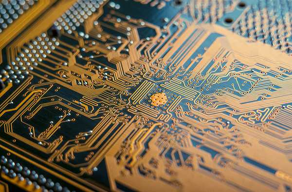
The printed circuit board (PCB) manufacturing industry has seen rapid technological advancements in recent years. PCBs are crucial components in nearly all modern electronics, from smartphones to aerospace systems. As electronics become more complex and miniaturized, PCB production methods must evolve to meet new challenges.
This article provides an overview of the latest PCB production technologies and innovations in 2023. We’ll examine new materials, precision manufacturing techniques, automation trends, and sustainability improvements shaping the industry. Whether you are a PCB designer, engineer, or manufacturer, understanding these advancements can help you make informed decisions about your next PCB project.
Key PCB Production Methods
There are several core methods used to manufacture PCBs:
Subtractive Processes
In subtractive processes, copper foil is laminated onto a blank fiberglass substrate. Unwanted copper is then etched away to leave only the desired circuit pattern. Common subtractive methods include:
- Chemical etching – Uses liquid etchants to dissolve away unwanted copper
- Plasma etching – Utilizes ionized gas plasma to ablate copper
- Mechanical milling – Machines like CNC routers literally mill away copper
Subtractive processes excel at high-volume production of simple PCBs. However, they generate substantial chemical waste and have limited resolution.
Additive Processes
Additive processes build up traces by selectively depositing conductive material onto the substrate. Common additive methods are:
- Electroplating – Uses electrical current to deposit copper onto seeded pattern
- Printed electronics – Directly prints conductive inks onto substrate
- Aerosol jet printing – Deposits ink through an aerosol spray
Additive processes are better for dense, complex PCBs like high-pin-count BGAs. They produce less waste but require advanced equipment.
Semi-Additive Processes
Semi-additive processes combine subtractive and additive steps. First, a thin copper foil is laminated. Desired traces are then electroplated to build up thickness. Finally, the original foil is etched away leaving only the plated traces.
Semi-additive offers a compromise between simplicity and resolution. It is the most common method used for mid-volume PCB production.
Hybrid Subtractive-Additive
Some advanced techniques use hybrid subtractive-additive processes. First, standard subtractive steps form the core traces. Then critical fine features are added using electroplating or direct print deposition.
This hybrid approach merges the benefits of both subtractive and additive, enabling high-density interconnects. However, it requires advanced equipment and process control.
Emerging PCB Materials and Substrates
The substrate material is the foundation upon which the PCB circuitry is built. The demands of new electronics have fueled research into novel substrates with enhanced properties.
Ceramic and Glass
Ceramic and glass substrates provide an ultra-stable and hermetic surface for building circuits. Ceramics offer high heat tolerance and low thermal expansion, making them ideal for rugged applications. Some common ceramic PCB substrates include:
- Alumina (Al2O3)
- Aluminum nitride (AlN)
- Silicon nitride (SiN)
Glass substrates have similar benefits to ceramics but cost less. Recent advances in laser drilling enable through-glass vias, allowing glass to replace traditional FR-4 in some applications.
Metal Core
Metal core PCBs contain a solid metal substrate instead of fiberglass. This allows direct LED or IC die attachment while also acting as a thermal heatsink. Aluminum, copper, and brass are common metal core substrates.
Flexible
Flexible PCBs use a polymer substrate that can bend and flex. Common flexible materials are polyimide, PEEK, and transparent conductive films. Wearables, medical devices, and consumer electronics utilize flexible PCBs for their mechanical compliance and durability.
HDI Technology
High-density interconnect (HDI) refers to technologies that enable tighter trace spacing and smaller vias. This allows more complex circuitry in a constrained footprint.
Microvias
Microvias are holes drilled in the PCB substrate with diameters under 150 microns. Laser drilling can produce microvias down to 50 microns for dense via patterns.
Thin Dielectrics
Using thinner dielectric build-up layers, often 25-50 microns, brings conductors closer together for fine lines and spaces. Thin laminates require advanced materials like expanded PTFE.
High Aspect Ratio Plating
High aspect ratio plating uses special chemistry to plate copper and fill via holes with heights up to 1:10 ratio. This allows microvias with pitches under 200 microns.
Sequential Lamination
Sequential lamination builds up thin HDI layers one at a time. This achieves up to 16-20 conductive layers, enabling high interconnect density.
Advanced PCB Finishes and Coatings
PCB finishes and coatings enhance solderability, corrosion resistance, and other surface properties.
Immersion Gold
Immersion gold finish is applied through a chemical displacement reaction. It offers excellent shelf life and wear resistance.
Electroless Nickel Immersion Gold (ENIG)
ENIG applies electroless nickel then immersion gold for a durable finish ideal for wire bonding.
Electroless Silver Immersion Gold (ESIG)
ESIG is similar to ENIG but using silver instead of nickel for optimal conductivity.
Electropalladium Nickel Gold (ENEPIG)
ENEPIG uses an electropalladium layer for excellent solderability and wire bondability.
Organic Solderability Preservatives (OSP)
OSP provides a temporary protective coating. It maintains solderability but has a short shelf life.
Conformal Coatings
Conformal coatings are polymeric films applied by dip or spray. They insulate boards from moisture, contamination, and corrosion.
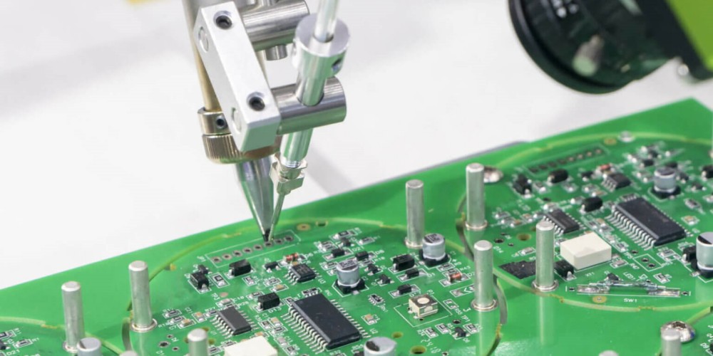
PCB Mass Production Automation
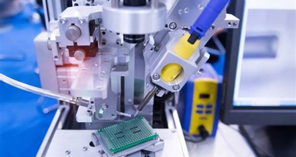
Achieving consistent high yields with complex PCBs requires extensive automation. Here are some examples:
Direct Imaging
Direct imaging uses laser light or charged particle beams to pattern resists. This eliminates physical photo tools.
Optical and X-ray Inspection
Automated optical inspection (AOI) and X-ray inspection quickly validates quality and detects defects.
Smart Warehouse Management
Inventory management systems track materials, improve planning, and prevent stock-outs.
Automated Testing
Electrical testing with flying probe testers or fixtures verifies continuity.
Smart Storage and Handling
Magazines, racks, and conveyors move boards reliably through production processes.
Sustainable Manufacturing Practices
Many PCB manufacturers are adopting greener production methods, including:
Renewable Energy
Use of solar, wind, and hydropower reduces the carbon footprint.
Chemical Waste Recycling
Systems to filter, reclaim, and reuse chemical etchants and plating solutions cut down on hazardous waste.
Lead-Free Processing
Lead-free soldering and fabrication eliminates risks from lead exposure.
Pollution Control
Air scrubbers, wastewater treatment, and fume extraction minimizes environmental impact.
RoHS Compliance
Following the EU’s Restriction of Hazardous Substances (RoHS) Directive restricts toxic chemicals.
Comparison of PCB Production Capabilities
| PCB Technology | Line Width | Via Size | Layers | Lead Time | Cost |
|---|---|---|---|---|---|
| Conventional FR4 | 125+ microns | 200+ microns | 16 max | 2-4 weeks | $ |
| HDI Any-Layer | 50 microns | 75 microns | 36 max | 4-6 weeks | $$ |
| Rigid-Flex | $$ | ||||
| Metal Core MCPCB | 2 max | 3-5 weeks | $$ | ||
| Ceramic/Glass | 50 microns | 50 microns | 30 max | 8-10 weeks | $$$ |
| Flex/Rigid-Flex | $$$ |
This table compares capabilities of common PCB production technologies. More advanced methods enable finer features but have longer lead times and higher costs.
Frequently Asked Questions
What are the latest PCB technology trends?
Some leading trends are HDI interconnects, flexible/rigid-flex boards, advanced finishing, and more sustainable processes. Additive and semi-additive methods are also increasing in usage.
What is the most advanced PCB technology?
Some of the most advanced technologies are sequential laminated multilayer processes with high-density interconnects, laser microvias, and thin dielectrics. This supports complex designs.
How small can PCB traces and spaces be made?
With HDI technology using thin dielectrics, laser-drilled microvias, and fine line photolithography, conductors with 25 micron lines and spaces are achievable.
Are ceramic PCBs better than FR4?
Ceramic PCBs offer higher performance and reliability thanks to excellent thermal and mechanical properties. But they cost far more than FR4 and have longer lead times.
What are the benefits of a metal core PCB?
Metal core PCBs allow direct die attachment for cooling and can serve as an EMI shield. The tradeoff is limited layer stackup compared to conventional laminates.


Leave a Reply