Introduction to PCBs
A printed circuit board (PCB) is a board used to mechanically support and electrically connect electronic components using conductive tracks, pads and other features. PCBs allow components to be interconnected without wires. They are used in almost all modern electronic devices.
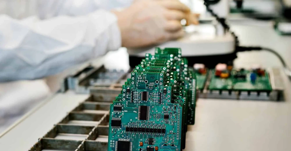
PCB processing refers to the manufacturing steps involved in creating a PCB from raw materials to finished board. It is a complex, multi-step process that requires high precision and quality control to produce functional boards. Understanding PCB processing helps designers, engineers and manufacturers optimize the process and identify potential issues.
This comprehensive guide provides an overview of key PCB processing steps, considerations and techniques used in fabrication.
PCB Design and Layout
PCB Design Software
The first step in PCB processing is design and layout using computer-aided design (CAD) software. Some common PCB design programs are:
- Altium Designer
- Cadence Allegro
- Mentor Graphics Xpedition
- Zuken CR-8000
These programs allow designers to virtually create schematics and PCB layouts with components and interconnects. Design rules and constraints are defined. The software outputs Gerber files, drill files, BOMs and other data needed for fabrication.
Layout Considerations
Some key layout factors affect manufacturability:
- Component placement – Parts should be positioned to optimize PCB real estate, routing, and efficiency. High-speed components require careful placement.
- Trace routing – Interconnect traces must be routed between pads while adhering to clearance rules. Autorouters can help optimize paths.
- Layer stackup – Layer count and order impacts size, cost and signal integrity. Four-layer boards are common. High-speed designs may need more layers.
- Via design – Vias connect traces between layers. Their size, quantity and placement affect signal quality.
- Ground planes – Continuous ground planes on inner layers enhance stability and EMI control. Split planes can isolate circuits.
- Finish and thickness – Immersion silver, ENIG and HASL are common finishes. Standard thickness is 1.6mm but can vary.
- Soldermask – Prevents solder bridging between pads while allowing soldering. LPI and LPS masks have tradeoffs.
- Silkscreen – Applied ink identifies components and branding. Should have adequate clearance from pads.
Careful layout is crucial for manufacturability and preventing assembly issues. Design for manufacturing (DFM) practices should be used.
Inner Layer Imaging
Inner layer processing forms the conductive copper traces on internal layers of a multilayer PCB. The key steps are:
Metallic Foil Application
Raw PCB laminate material is coated with a thin sheet of copper foil, typically 0.5-2 oz. Roller coating, electroplating or gluing methods adhere foil uniformly across each layer. The foil thickness determines trace impedance.
Photoresist Lamination
A layer of liquid photoresist is applied over the copper foil. Photoresist is a light-sensitive epoxy that will form a mask during etching. Lamination ensures uniform photoresist thickness.
Exposure
The photoresist is selectively exposed to UV light through a photographic mask, hardening exposed areas. Masks are produced from Gerber files and block light where traces will remain.
Developing
The PCB panel goes through a chemical developing bath which dissolves away unexposed photoresist. This leaves a pattern of hardened photoresist matching the circuit trace layout.
Etching
Etchant chemicals are sprayed or immersed to eat away unwanted copper not protected by photoresist. Common etchants are ferric chloride and ammonium persulfate. Etching leaves only desired conductor traces under the photoresist.
Stripping
Once etching is complete, the remaining photoresist is chemically stripped away, revealing the finished conductive pattern. An anti-tarnishing treatment is sometimes applied to protect exposed copper.
These steps are repeated for each inner layer. Alignment is critical to ensure vias connect properly between layers. High accuracy phototools and imaging equipment is used.
Layer Stack and Alignment
The inner layer cores are aligned and the full layer stack is assembled prior to lamination.
- Dummy layers may fill the stack if an odd layer count is needed.
- Core layers are cleaned then inspected for defects and debris.
- Layers are precisely aligned using registration holes or fiducials.
- The stack is tacked together using adhesive dots, pins or clamps.
- Additional foils or metal sheets may be added to the stack.
Maintaining alignment tolerance throughout lamination is critical, often held to within 0.1mm.
Lamination
Lamination fuses together the layers of a PCB into a single unified board by applying heat and pressure:
- The layer stack assembly is loaded into a lamination press.
- Sheets of prepreg bonding material are added between each layer. Prepreg is B-stage epoxy resin.
- Heat up to 180°C and pressure around 1000 psi is applied for over an hour to fully cure bonding layers.
- Excess resin and voids are squeezed out, leaving a solid laminate.
- Multi-opening presses can laminate multiple boards simultaneously.
- Some flex and rigid-flex boards require sequential lamination.
- Cooling under pressure prevents warping.
High temperatures and precise lamination control prevent inner layer movement or distortion. Lamination quality determines long-term PCB reliability.
Outer Layer Imaging
After lamination, a similar photolithographic process is used to image outer layers.
First, a layer of copper foil is laminated onto both outer surfaces of the PCB core. Photoresist is applied, exposed through the soldermask pattern, and developed. The board is etched to form the soldermask openings, fusing pads and traces to the laminated foil.
For double-sided boards, this completes processing. For multilayer boards, surface finishes and soldermask are still required.
Surface Finishes
PCBs are plated with metallic surface finishes to protect exposed copper traces and enhance soldering:
- Hot air solder leveling (HASL) applies a solder coating which completely covers copper. Provides good solderability but can cause tin whiskers.
- Electroless Nickel Immersion Gold (ENIG) deposits a nickel barrier layer and thin gold coat. Provides excellent solderability but higher cost.
- Immersion Silver coats traces in a thin layer of silver. Lower cost but more prone to oxidation.
- Organic Solderability Preservatives (OSP) coat copper to prevent oxidation and improve soldering.
The optimal finish depends on soldering process, cost and reliability requirements. Common finishes are ENIG, HASL and Immersion Silver.
Soldermask Application
The soldermask serves as a protective insulator preventing solder bridges from forming between traces. It is typically dark green.
There are two approaches:
- LPI (Liquid PhotoImageable) soldermask is applied as a thick liquid epoxy. It is exposed and cured into permanent openings surrounding pads and traces.
- LPS (Laser Direct Structuring) is applied as a uniform dry film. Openings are ablated into the mask with a laser.
LPI allows finer precision but LPS has fewer steps. Soldermask registration can compensate for inner layer misalignment. Global coating ensures adequate dielectric isolation.
Silkscreen Printing
Silkscreen printing applies epoxy-based ink onto the PCB to print component outlines, markings, branding logos and identification. Printed legends must allow adequate clearance from pads and traces. Screens and thick-film inks produce a permanent markings and labels.
Solder Paste Stencils
Solder paste stencils are thin metal masks laser cut to match the PCB’s pad and opening pattern. These are used to apply precise patterned solder paste deposits onto the board for surface mount component placement. Stencils are considered part of the PCB fabrication process.
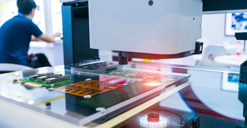
Electrical Testing
Once fully processed, PCBs undergo electrical testing:
- Automated optical inspection looks for defects in trace width, spacing, and coating registration.
- Flying probe or bed-of-nails fixtures test electrical connectivity and shorts between nodes.
- Impedance testing validates controlled impedance traces match requirements.
- Functional testing verifies boards operate correctly.
Testing helps screen out defective PCBs prior to shipment and assembly.
Final Processing
Final steps prepare the finished boards for shipping:
- Visual inspection under magnification checks for defects. Automatic optical inspection is also used.
- Boards are depanelized by breaking V-score lines or using a router. Individual PCB units are separated.
- Conformal coating can be applied to enhance environmental protection.
- Boards are packed and shipped using anti-static materials to prevent ESD damage.
Thorough processing and quality checks help ensure customers receive fully functional and reliable PCBs.
Benefits of Outsourcing PCB Production
Many companies outsource PCB fabrication to dedicated production facilities in order to focus internal efforts on design and avoid capital costs. Here are some benefits of outsourcing:
- Cost savings – No need to purchase expensive PCB fabrication equipment and employ specialized staff to maintain production lines. Outsourcing converts fixed costs into a variable cost.
- Focus on core competencies – Lets companies concentrate on design and engineering rather than manufacturing. Outsourcing simplifies business operations.
- Access to advanced technology – Leading PCB manufacturers continuously upgrade equipment. Outsourcing provides access to the latest fabrication techniques.
- Flexible production capacity – Output can be scaled easily based on changing demand. No need to add additional lines.
- Reduced time-to-market – Outsourcing speeds up manufacturing lead times for quicker product launch.
- Quality and yields – Experienced manufacturers have refined processes to achieve high yields and reliability. Their expertise improves quality.
However, companies must carefully qualify and audit outsourced vendors to ensure stringent standards are upheld. Legal protections like NDAs safeguard proprietary designs and technologies.
Selecting a PCB Manufacturer
Here are key factors to consider when selecting a PCB production partner:
Capabilities and Offerings
- Available PCB technologies – Determine if the vendor can support required board types like HDI, rigid-flex or heavy copper boards.
- Board materials – Assess capabilities with required substrate materials like FR-4, polyimide, ceramic or PTFE.
- Layers – Evaluate whether shop can produce needed layer counts. High layer count PCBs often require specialized equipment.
- Board size – Verify manufacturer can accommodate maximum PCB dimensions without cutting panels.
- Volume production – Choose a vendor equipped for required quantities, from small prototypes to longer production runs.
- Design restrictions – Check for any unique DFM rules or design constraints imposed by the vendor’s process.
- Certifications – Look for ISO-9001 compliance and other applicable quality certifications.
- Supply chain management – Evaluate processes for sourcing raw PCB materials and component supply.
- Value-added services – Services like assembly, testing and box build can simplify production.
Process and Quality
- Facilities – Visit sites if possible to inspect equipment, operations and quality control.
- Process controls – Review procedures for configuration management, change control and process repeatability.
- Inspection – Learn about automated optical, electrical, and functional testing performed.
- Quality metrics – Assess process capability index metrics like Cpk and production yields.
- Continual improvement – Look for efforts to refine methods and reduce defects. Kaizen events help engrain quality culture.
- ESD control – Evaluate ESD safeguards like grounded equipment, wrist straps and packaging.
- Traceability – Verify PCB lots and components can be traced back to suppliers and production records.
Experience and Expertise
- Years in business – Longer history indicates stable production expertise. Newer shops may lack experience.
- Staff expertise – Evaluate technical expertise of engineering, production and quality assurance staff.
- Industry certifications – Relevant qualifications like IPC-A-610 demonstrate focused PCB assembly training.
- Customer base – Varied industries and customer longevity demonstrate flexible expertise.
- Technical support – Assessity of engineering support for design reviews and troubleshooting issues.
- Continuous improvement – Vendor should demonstrate commitment to improving methods and skills through training.
Carefully vet potential PCB partners on these criteria to find the best match for manufacturing needs and product quality goals.
Common PCB Defects
Despite stringent quality control, defects can occur during PCB fabrication and lead to boards failing either during production or once assembled:
Physical Defects
- Voids – Empty pockets or gaps in dielectric layers caused by incomplete resin filling during lamination. Can reduce voltage isolation.
- Craters – Pits and dents in copper traces from over-etching. Can impact conductance.
- Copper wicking – Etchant seeping under photoresist causes reduced trace width and impedance issues.
- Burrs – Rough copper edges or nodules protruding from traces. Problematic for HDI.
- Delamination – Laminate separating due to poor adhesion between layers or thermal stress.
- Warping – Improper cooling after lamination results in bowed or twisted boards.
Pattern Defects
- Open circuits – Missing or broken conductor path preventing current flow.
- Short circuits – Unintended connection between nodes, often from excess copper.
- Spurious copper – Unwanted copper remnants creating shorts, often under components.
- Registration errors – Misalignment between layers places vias off target.
- Wrong hole size – Drilled holes differ from design. Can impact fit with components.
- Clearance violations – Insufficient spacing between adjacent copper features. Raises shorting risk.
Component Defects
- Missing parts – Omitted components due to assembly errors.
- Incorrect parts – Wrong parts populated on board.
- Misorientations – Components placed in improper orientation.
- Shifted parts – Components shifted from intended location.
- Incorrect values – Wrong value components installed.
- Solder defects – Cold joints, bridges or insufficient solder.
Inspecting fabricated boards and performing electrical testing helps eliminate potential defects before shipment. Production monitoring, maintenance and staff training minimizes defects.
PCB Process Monitoring and Control
Consistent quality requires continuously monitoring fabrication processes and employing statistical process control (SPC). Common techniques include:
In-Process Inspection
- Automated optical inspection after photolithography stages captures physical and pattern defects.
- Lamimate integrity tests like cross-section microscopic inspection and mechanical testing check for flaws.
- Soldermask thickness measurement ensures uniformity.
- Impedance testing validates controlled impedance traces match requirements.
- Plating thickness measurement confirms proper conductor thickness.
Sampling
- Test coupons fabricated with production panels enable off-line quality testing without destroying salable boards.
- Sample lots taken from production runs are electrically tested. Failures indicate process issues.
- Scrap analysis examines defect root causes by type and frequency.
- SEM cross-sections of samples check for sub-surface flaws under traces.
Process Monitoring
- Records log machine parameters, test results and environmental conditions traceable by job and lot.
- SPC charts plot key parameters statistically with upper and lower control limits to identify deviations.
- Traceability through production data and serial numbers enables tracking components to finished boards.
- Maintenance prevents equipment wear and drift. Regular calibration ensures reliability.
Corrective Actions
- Process adjustments address parameters moving outside control limits before producing defects.
- Troubleshooting identifies root cause of defects using Pareto, fishbone diagram and 5 Whys analysis.
- Preventive measures implement fixes and improvement plans based on data.
- Staff communication and training aim to avoid repeating errors.
Continuous process control, corrective action and improvement ensure optimal PCB quality over the long-term.
FQA on PCB Processing
What are some key considerations during PCB layout and design?
Some important layout considerations are component placement for efficiency and routing, trace routing to meet clearance requirements, layer stackup configuration to balance cost and performance, via design impacting signal quality, ground planes for stability, finish and thickness values, soldermask effect on bridging, and adequate silkscreen clearance from pads. Following design for manufacturing (DFM) rules helps maximize manufacturability.
What is the purpose of a solder paste stencil in PCB assembly?
Solder paste stencils are thin metal masks laser cut to match the PCB’s pad and soldermask opening pattern. During assembly, solder paste is deposited through the stencil onto pads on the PCB. This provides precise, controlled amounts of solder paste where components will be placed for surface mount soldering. The stencil enables accurate and repeatable solder paste application.
What are some common PCB surface finishes?
Common metallic PCB surface finishes include:
- Hot air solder leveling (HASL) which applies a solder coating
- Electroless Nickel Immersion Gold (ENIG) which plates a nickel barrier and thin gold coat
- Immersion silver coating the traces in silver
- Organic Solderability Preservatives (OSP) that coat copper to prevent oxidation
The optimal finish depends on soldering process requirements, cost, longevity and performance needs. ENIG, HASL and immersion silver are widely used.
What are some key factors when selecting a PCB manufacturing partner?
Important selection factors are capabilities to produce required board technologies, sizes and volumes, materials used, quality certifications, process controls, manufacturing facilities and conditions, inspection procedures, staff expertise and experience, customer base, technical support, and continual improvement commitment. The best match depends on product needs, quality goals and working relationship dynamics.
What are common causes of PCB delamination failures
PCB Processing: A Comprehensive Guide
Introduction to PCBs
A printed circuit board (PCB) is a board used to mechanically support and electrically connect electronic components using conductive tracks, pads and other features. PCBs allow components to be interconnected without wires. They are used in almost all modern electronic devices.
PCB processing refers to the manufacturing steps involved in creating a PCB from raw materials to finished board. It is a complex, multi-step process that requires high precision and quality control to produce functional boards. Understanding PCB processing helps designers, engineers and manufacturers optimize the process and identify potential issues.
This comprehensive guide provides an overview of key PCB processing steps, considerations and techniques used in fabrication.
PCB Design and Layout
PCB Design Software
The first step in PCB processing is design and layout using computer-aided design (CAD) software. Some common PCB design programs are:
- Altium Designer
- Cadence Allegro
- Mentor Graphics Xpedition
- Zuken CR-8000
These programs allow designers to virtually create schematics and PCB layouts with components and interconnects. Design rules and constraints are defined. The software outputs Gerber files, drill files, BOMs and other data needed for fabrication.
Layout Considerations
Some key layout factors affect manufacturability:
- Component placement – Parts should be positioned to optimize PCB real estate, routing, and efficiency. High-speed components require careful placement.
- Trace routing – Interconnect traces must be routed between pads while adhering to clearance rules. Autorouters can help optimize paths.
- Layer stackup – Layer count and order impacts size, cost and signal integrity. Four-layer boards are common. High-speed designs may need more layers.
- Via design – Vias connect traces between layers. Their size, quantity and placement affect signal quality.
- Ground planes – Continuous ground planes on inner layers enhance stability and EMI control. Split planes can isolate circuits.
- Finish and thickness – Immersion silver, ENIG and HASL are common finishes. Standard thickness is 1.6mm but can vary.
- Soldermask – Prevents solder bridging between pads while allowing soldering. LPI and LPS masks have tradeoffs.
- Silkscreen – Applied ink identifies components and branding. Should have adequate clearance from pads.
Careful layout is crucial for manufacturability and preventing assembly issues. Design for manufacturing (DFM) practices should be used.
Inner Layer Imaging
Inner layer processing forms the conductive copper traces on internal layers of a multilayer PCB. The key steps are:
Metallic Foil Application
Raw PCB laminate material is coated with a thin sheet of copper foil, typically 0.5-2 oz. Roller coating, electroplating or gluing methods adhere foil uniformly across each layer. The foil thickness determines trace impedance.
Photoresist Lamination
A layer of liquid photoresist is applied over the copper foil. Photoresist is a light-sensitive epoxy that will form a mask during etching. Lamination ensures uniform photoresist thickness.
Exposure
The photoresist is selectively exposed to UV light through a photographic mask, hardening exposed areas. Masks are produced from Gerber files and block light where traces will remain.
Developing
The PCB panel goes through a chemical developing bath which dissolves away unexposed photoresist. This leaves a pattern of hardened photoresist matching the circuit trace layout.
Etching
Etchant chemicals are sprayed or immersed to eat away unwanted copper not protected by photoresist. Common etchants are ferric chloride and ammonium persulfate. Etching leaves only desired conductor traces under the photoresist.
Stripping
Once etching is complete, the remaining photoresist is chemically stripped away, revealing the finished conductive pattern. An anti-tarnishing treatment is sometimes applied to protect exposed copper.
These steps are repeated for each inner layer. Alignment is critical to ensure vias connect properly between layers. High accuracy phototools and imaging equipment is used.
Layer Stack and Alignment
The inner layer cores are aligned and the full layer stack is assembled prior to lamination.
- Dummy layers may fill the stack if an odd layer count is needed.
- Core layers are cleaned then inspected for defects and debris.
- Layers are precisely aligned using registration holes or fiducials.
- The stack is tacked together using adhesive dots, pins or clamps.
- Additional foils or metal sheets may be added to the stack.
Maintaining alignment tolerance throughout lamination is critical, often held to within 0.1mm.
Lamination
Lamination fuses together the layers of a PCB into a single unified board by applying heat and pressure:
- The layer stack assembly is loaded into a lamination press.
- Sheets of prepreg bonding material are added between each layer. Prepreg is B-stage epoxy resin.
- Heat up to 180°C and pressure around 1000 psi is applied for over an hour to fully cure bonding layers.
- Excess resin and voids are squeezed out, leaving a solid laminate.
- Multi-opening presses can laminate multiple boards simultaneously.
- Some flex and rigid-flex boards require sequential lamination.
- Cooling under pressure prevents warping.
High temperatures and precise lamination control prevent inner layer movement or distortion. Lamination quality determines long-term PCB reliability.
Outer Layer Imaging
After lamination, a similar photolithographic process is used to image outer layers.
First, a layer of copper foil is laminated onto both outer surfaces of the PCB core. Photoresist is applied, exposed through the soldermask pattern, and developed. The board is etched to form the soldermask openings, fusing pads and traces to the laminated foil.
For double-sided boards, this completes processing. For multilayer boards, surface finishes and soldermask are still required.
Surface Finishes
PCBs are plated with metallic surface finishes to protect exposed copper traces and enhance soldering:
- Hot air solder leveling (HASL) applies a solder coating which completely covers copper. Provides good solderability but can cause tin whiskers.
- Electroless Nickel Immersion Gold (ENIG) deposits a nickel barrier layer and thin gold coat. Provides excellent solderability but higher cost.
- Immersion Silver coats traces in a thin layer of silver. Lower cost but more prone to oxidation.
- Organic Solderability Preservatives (OSP) coat copper to prevent oxidation and improve soldering.
The optimal finish depends on soldering process, cost and reliability requirements. Common finishes are ENIG, HASL and Immersion Silver.
Soldermask Application
The soldermask serves as a protective insulator preventing solder bridges from forming between traces. It is typically dark green.
There are two approaches:
- LPI (Liquid PhotoImageable) soldermask is applied as a thick liquid epoxy. It is exposed and cured into permanent openings surrounding pads and traces.
- LPS (Laser Direct Structuring) is applied as a uniform dry film. Openings are ablated into the mask with a laser.
LPI allows finer precision but LPS has fewer steps. Soldermask registration can compensate for inner layer misalignment. Global coating ensures adequate dielectric isolation.
Silkscreen Printing
Silkscreen printing applies epoxy-based ink onto the PCB to print component outlines, markings, branding logos and identification. Printed legends must allow adequate clearance from pads and traces. Screens and thick-film inks produce a permanent markings and labels.
Solder Paste Stencils
Solder paste stencils are thin metal masks laser cut to match the PCB’s pad and opening pattern. These are used to apply precise patterned solder paste deposits onto the board for surface mount component placement. Stencils are considered part of the PCB fabrication process.
Electrical Testing
Once fully processed, PCBs undergo electrical testing:
- Automated optical inspection looks for defects in trace width, spacing, and coating registration.
- Flying probe or bed-of-nails fixtures test electrical connectivity and shorts between nodes.
- Impedance testing validates controlled impedance traces match requirements.
- Functional testing verifies boards operate correctly.
Testing helps screen out defective PCBs prior to shipment and assembly.
Final Processing
Final steps prepare the finished boards for shipping:
- Visual inspection under magnification checks for defects. Automatic optical inspection is also used.
- Boards are depanelized by breaking V-score lines or using a router. Individual PCB units are separated.
- Conformal coating can be applied to enhance environmental protection.
- Boards are packed and shipped using anti-static materials to prevent ESD damage.
Thorough processing and quality checks help ensure customers receive fully functional and reliable PCBs.
Benefits of Outsourcing PCB Production
Many companies outsource PCB fabrication to dedicated production facilities in order to focus internal efforts on design and avoid capital costs. Here are some benefits of outsourcing:
- Cost savings – No need to purchase expensive PCB fabrication equipment and employ specialized staff to maintain production lines. Outsourcing converts fixed costs into a variable cost.
- Focus on core competencies – Lets companies concentrate on design and engineering rather than manufacturing. Outsourcing simplifies business operations.
- Access to advanced technology – Leading PCB manufacturers continuously upgrade equipment. Outsourcing provides access to the latest fabrication techniques.
- Flexible production capacity – Output can be scaled easily based on changing demand. No need to add additional lines.
- Reduced time-to-market – Outsourcing speeds up manufacturing lead times for quicker product launch.
- Quality and yields – Experienced manufacturers have refined processes to achieve high yields and reliability. Their expertise improves quality.
However, companies must carefully qualify and audit outsourced vendors to ensure stringent standards are upheld. Legal protections like NDAs safeguard proprietary designs and technologies.
Selecting a PCB Manufacturer
Here are key factors to consider when selecting a PCB production partner:
Capabilities and Offerings
- Available PCB technologies – Determine if the vendor can support required board types like HDI, rigid-flex or heavy copper boards.
- Board materials – Assess capabilities with required substrate materials like FR-4, polyimide, ceramic or PTFE.
- Layers – Evaluate whether shop can produce needed layer counts. High layer count PCBs often require specialized equipment.
- Board size – Verify manufacturer can accommodate maximum PCB dimensions without cutting panels.
- Volume production – Choose a vendor equipped for required quantities, from small prototypes to longer production runs.
- Design restrictions – Check for any unique DFM rules or design constraints imposed by the vendor’s process.
- Certifications – Look for ISO-9001 compliance and other applicable quality certifications.
- Supply chain management – Evaluate processes for sourcing raw PCB materials and component supply.
- Value-added services – Services like assembly, testing and box build can simplify production.
Process and Quality
- Facilities – Visit sites if possible to inspect equipment, operations and quality control.
- Process controls – Review procedures for configuration management, change control and process repeatability.
- Inspection – Learn about automated optical, electrical, and functional testing performed.
- Quality metrics – Assess process capability index metrics like Cpk and production yields.
- Continual improvement – Look for efforts to refine methods and reduce defects. Kaizen events help engrain quality culture.
- ESD control – Evaluate ESD safeguards like grounded equipment, wrist straps and packaging.
- Traceability – Verify PCB lots and components can be traced back to suppliers and production records.
Experience and Expertise
- Years in business – Longer history indicates stable production expertise. Newer shops may lack experience.
- Staff expertise – Evaluate technical expertise of engineering, production and quality assurance staff.
- Industry certifications – Relevant qualifications like IPC-A-610 demonstrate focused PCB assembly training.
- Customer base – Varied industries and customer longevity demonstrate flexible expertise.
- Technical support – Assessity of engineering support for design reviews and troubleshooting issues.
- Continuous improvement – Vendor should demonstrate commitment to improving methods and skills through training.
Carefully vet potential PCB partners on these criteria to find the best match for manufacturing needs and product quality goals.
Common PCB Defects
Despite stringent quality control, defects can occur during PCB fabrication and lead to boards failing either during production or once assembled:
Physical Defects
- Voids – Empty pockets or gaps in dielectric layers caused by incomplete resin filling during lamination. Can reduce voltage isolation.
- Craters – Pits and dents in copper traces from over-etching. Can impact conductance.
- Copper wicking – Etchant seeping under photoresist causes reduced trace width and impedance issues.
- Burrs – Rough copper edges or nodules protruding from traces. Problematic for HDI.
- Delamination – Laminate separating due to poor adhesion between layers or thermal stress.
- Warping – Improper cooling after lamination results in bowed or twisted boards.
Pattern Defects
- Open circuits – Missing or broken conductor path preventing current flow.
- Short circuits – Unintended connection between nodes, often from excess copper.
- Spurious copper – Unwanted copper remnants creating shorts, often under components.
- Registration errors – Misalignment between layers places vias off target.
- Wrong hole size – Drilled holes differ from design. Can impact fit with components.
- Clearance violations – Insufficient spacing between adjacent copper features. Raises shorting risk.
Component Defects
- Missing parts – Omitted components due to assembly errors.
- Incorrect parts – Wrong parts populated on board.
- Misorientations – Components placed in improper orientation.
- Shifted parts – Components shifted from intended location.
- Incorrect values – Wrong value components installed.
- Solder defects – Cold joints, bridges or insufficient solder.
Inspecting fabricated boards and performing electrical testing helps eliminate potential defects before shipment. Production monitoring, maintenance and staff training minimizes defects.
PCB Process Monitoring and Control
Consistent quality requires continuously monitoring fabrication processes and employing statistical process control (SPC). Common techniques include:
In-Process Inspection
- Automated optical inspection after photolithography stages captures physical and pattern defects.
- Lamimate integrity tests like cross-section microscopic inspection and mechanical testing check for flaws.
- Soldermask thickness measurement ensures uniformity.
- Impedance testing validates controlled impedance traces match requirements.
- Plating thickness measurement confirms proper conductor thickness.
Sampling
- Test coupons fabricated with production panels enable off-line quality testing without destroying salable boards.
- Sample lots taken from production runs are electrically tested. Failures indicate process issues.
- Scrap analysis examines defect root causes by type and frequency.
- SEM cross-sections of samples check for sub-surface flaws under traces.
Process Monitoring
- Records log machine parameters, test results and environmental conditions traceable by job and lot.
- SPC charts plot key parameters statistically with upper and lower control limits to identify deviations.
- Traceability through production data and serial numbers enables tracking components to finished boards.
- Maintenance prevents equipment wear and drift. Regular calibration ensures reliability.
Corrective Actions
- Process adjustments address parameters moving outside control limits before producing defects.
- Troubleshooting identifies root cause of defects using Pareto, fishbone diagram and 5 Whys analysis.
- Preventive measures implement fixes and improvement plans based on data.
- Staff communication and training aim to avoid repeating errors.
Continuous process control, corrective action and improvement ensure optimal PCB quality over the long-term.
FQA on PCB Processing
What are some key considerations during PCB layout and design?
Some important layout considerations are component placement for efficiency and routing, trace routing to meet clearance requirements, layer stackup configuration to balance cost and performance, via design impacting signal quality, ground planes for stability, finish and thickness values, soldermask effect on bridging, and adequate silkscreen clearance from pads. Following design for manufacturing (DFM) rules helps maximize manufacturability.
What is the purpose of a solder paste stencil in PCB assembly?
Solder paste stencils are thin metal masks laser cut to match the PCB’s pad and soldermask opening pattern. During assembly, solder paste is deposited through the stencil onto pads on the PCB. This provides precise, controlled amounts of solder paste where components will be placed for surface mount soldering. The stencil enables accurate and repeatable solder paste application.
What are some common PCB surface finishes?
Common metallic PCB surface finishes include:
- Hot air solder leveling (HASL) which applies a solder coating
- Electroless Nickel Immersion Gold (ENIG) which plates a nickel barrier and thin gold coat
- Immersion silver coating the traces in silver
- Organic Solderability Preservatives (OSP) that coat copper to prevent oxidation
The optimal finish depends on soldering process requirements, cost, longevity and performance needs. ENIG, HASL and immersion silver are widely used.
What are some key factors when selecting a PCB manufacturing partner?
Important selection factors are capabilities to produce required board technologies, sizes and volumes, materials used, quality certifications, process controls, manufacturing facilities and conditions, inspection procedures, staff expertise and experience, customer base, technical support, and continual improvement commitment. The best match depends on product needs, quality goals and working relationship dynamics.


Leave a Reply