What is PCB Printing?
Printed circuit boards (PCBs) are the foundation of modern electronics. A PCB mechanically supports and electrically connects electronic components using conductive tracks, pads and other features etched from one or more sheet layers of copper laminated onto and/or between sheet layers of a non-conductive substrate. PCBs can be simple, single-sided circuit boards or complex multilayer boards.
The process of manufacturing PCBs is called PCB fabrication. It involves taking the PCB design files and printing the board layer by layer using a variety of specialized techniques. In this guide, we’ll explore the step-by-step PCB printing process, from design to finished board.
The PCB Printing Process
While the details vary between PCB manufacturers, the general PCB printing process follows these key steps:
1. Design
Engineers create the PCB design files using CAD (computer-aided design) software. The PCB layout will include the component footprints, trace routing, drill holes, copper fills, and other features. Popular PCB design software packages include Altium Designer, Eagle, KiCad, and OrCAD.
The CAD files are exported in standard formats like Gerber files, drill files, netlists, etc. These files provide all the information needed for PCB printing.
2. Pre-Production Checks
The PCB manufacturer will import the CAD data and run design rule checks to validate the manufacturability of the board. This verifies features are within capabilities, there are no errors like trace width violations or annular ring violations, etc.
If errors are found, they will request the customer resubmit corrected design files.
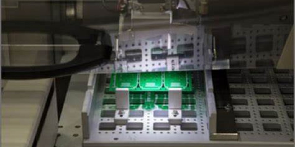
3. Inner Layer Production
Most PCBs have multiple conductive copper layers separated by dielectric substrate layers. The inner layers are produced first in a press process.
- Substrate Material: Common rigid PCB substrate materials include FR-4 glass epoxy and high-frequency PTFE. The substrate comes pre-coated with copper foil.
- Photoresist Application: A photosensitive resist material is applied over the copper foil. This can be liquid or dry film.
- Imaging: Using lithography techniques, the PCB design pattern is imaged onto each inner layer. This selectively exposes areas of the photoresist.
- Developing: The resist is developed, removing either exposed or unexposed areas. This leaves behind a patterned resist mask.
- Etching: Etchants dissolve away copper not protected by resist. This transfers the PCB trace pattern to the inner layers.
- Resist Strip: Remaining photoresist is removed, leaving just the desired copper pattern on the inner layers
- Layer Alignment: Inner layers are precisely aligned and laminated together into a multilayer board stackup.
4. Outer Layer Processing
The outer layer copper features are formed on the assembled board stackup using similar lithographic processes. This builds up the outer layer circuitry, completing the PCB layer construction.
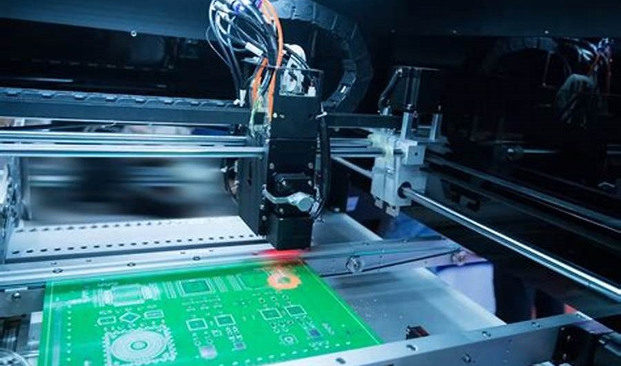
5. Drilling
Using the drill files from the CAD data, holes are drilled through the board to connect layers electrically and allow component attachment. High-speed CNC drill machines produce extremely precise holes.
6. Plating and Coating
- Via Plating: The drilled holes are electroplated to coat the interior walls with copper, forming a conductive via between layers.
- Panel Plating: The entire board surface is plated to increase copper thickness for conductors.
- Soldermask: A lacquer layer is screened and patterned onto both outer surfaces of the PCB panel. This protects copper traces from oxidation and prevents solder bridging between pads.
- Silkscreen: Printed text and markings are screened onto the soldermask to identify components, contacts, branding logos, etc.
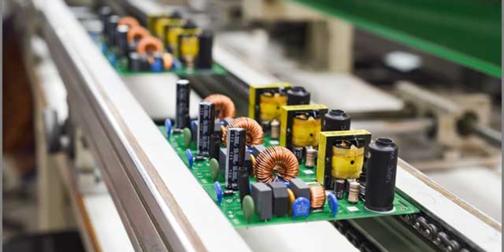
7. Final Processing
- Solder Paste Stencils: Laser cut metal stencils are made to apply solder paste for SMT components during assembly.
- Routing: A router machine cuts the panel into individual PCBs. Slots, cutouts, chamfers, etc. are routed as needed.
- Testing: Quality assurance testing like netlist continuity test, AOI, and functional test are conducted.
- Packaging: Boards are inspected, baked, and packed to ship to customer.
PCB Printing Techniques
There are a few dominant PCB printing techniques used in fabrication:
Subtractive Process
The subtractive process starts with a copper clad laminate and etches away (subtracts) material to form the traces. This is the most common PCB printing approach and used for over 90% of rigid PCBs produced today.
Advantages include:
- Mature, well-understood process
- Excellent fine line/space capabilities
- Tight control of trace geometries
- Good for high-density designs
- Cost-effective
Disadvantages:
- Generates chemical waste streams
- Limited in high aspect ratio and thick metal capabilities
Additive Process
With additive processing, traces are selectively built up on the substrate. A common additive approach is semi-additive:
- Start with unclad substrate
- Full panel metallization
- Print resist pattern
- Electroplate copper on exposed areas
- Strip resist
Advantages:
- No etching chemicals
- Plating resists provide high aspect ratio traces
- Suitable for ultra-HDI PCBs
Disadvantages:
- More process steps
- Tighter process controls needed
- Only recently adopted at large scale
Modified Semi-Additive Process
Modified semi-additive combines aspects of subtractive and additive for improved capabilities:
- Start with thin copper foil
- Pattern plate thicker copper traces
- Etch foil removing field copper
Offers advantages of both while minimizing disadvantages.
Printed Electronics
Printed electronics methods like inkjet and aerosol printing are additive, maskless processes. Conductive and resistive inks are deposited directly. Lower resolution than other processes but useful for simpler circuits.
Other Methods
Some other niche PCB printing methods include:
- Photolithography
- Laser direct imaging
- 3D printing
- Electrochemical machining
PCB Printing Capabilities
PCB printing techniques enable fabrication of boards with the following capabilities:
Line Width and Spacing
The smallest printed line width and spacing that can be achieved. Determines PCB density.
| Type | Width/Spacing |
|---|---|
| Class 2 | ≥ 6 mil |
| Class 3 | ≥ 4 mil |
| Class 4 | ≥ 2 mil |
Via Sizes and Density
How small and closely-spaced drilled vias can be fabricated. Important for HDI boards.
| Type | Drilled Via | Microvia |
|---|---|---|
| Low-density | ≥ 8 mil diameter | NA |
| Medium-density | ≥ 5 mil diameter | ≥ 0.2 mm pitch |
| High-density | ≥ 4 mil diameter | ≥ 0.1 mm pitch |
Layer Count
Number of conductive copper layers in the PCB. More layers accommodates complex routing.
- 2 to 6 layers: Low-density consumer PCBs
- 8 to 14 layers: Mid-density boards
- 16+ layers: High-density boards like advanced telecom and networking
Pad and Hole Sizes
Smallest printed pad diameters and drilled hole sizes.
- Minimum pad diameter: 4-6 mil
- Minimum plated through hole: 4-6 mil
Finest Line Roughness
Small variations in trace edges. Affects high speed signal integrity.
- Subtractive etching: Higher roughness
- Additive plating: Lower roughness
Registration Accuracy
How precisely layers align. 0.5 mil typical for primary alignment.
Conductor Thickness
- Subtractive 1/2 oz (0.7 mils) typical but can be heavier
- Additive/Semi-additive up to 2-3 oz (2.8 – 4.2 mils)
PCB Printing Applications
PCB printing techniques are used to produce boards for nearly every electronics subfield, including:
- Consumer electronics
- Computers and peripherals
- Communications infrastructure
- Automotive electronics
- Aerospace and defense
- Medical devices
- Industrial equipment
And many more. Different applications have specialized PCB requirements that the fabrication process must meet.
Pros and Cons of PCB Printing
Here are some key advantages and disadvantages of printed circuit boards:
Pros
- Enable dense, complex electronics packaging
- Extremely consistent and repeatable
- Mature, high-volume mass production
- Faster and lower cost than point-to-point wiring
- Facilitates automated component assembly
Cons
- Design complexity and long iterative process
- Upfront cost for prototype low volume
- Difficult to modify or repair after production
- Long lead times for manufacturing
- Some chemical waste generated (subtractive)
The Future of PCB Printing
Engineers continue advancing PCB technology through innovations like:
- Additive methods for higher density traces
- Lower-loss, higher-frequency substrate materials
- Embedded components for further miniaturization
- 3D printing of boards with high aspect ratio features
- Advanced testing and inspection techniques
This allows increased functionality and capabilities for emerging applications. The PCB serves as the foundation enabling the electronics innovations of tomorrow.
Frequently Asked Questions
What are the main steps in PCB printing?
The main steps are design, pre-production checks, inner layer production, outer layer processing, drilling, plating/coating, final processing, and testing. This transforms the PCB from CAD design files into fabricated boards.
How are traces printed onto the PCB substrate?
Traces are formed by either a subtractive or additive process. Subtractive uses etching to remove unwanted copper. Additive plates or prints trace material directly onto the substrate.
What minimum line width and spacing can PCB printing achieve?
The finest PCB printing can produce 2 mil wide traces and spaces. This supports high-density class 4 PCB designs.
How many conductive layers can modern PCBs have?
High-density boards used in advanced electronics can have 16 or more layers. Simple consumer PCBs often use just 2 to 4 layers.
How are holes drilled in PCBs?
A CNC drill machine drills holes precisely placed according to the CAD drill files. These holes are then electroplated to form conductive vias between layers.


Leave a Reply