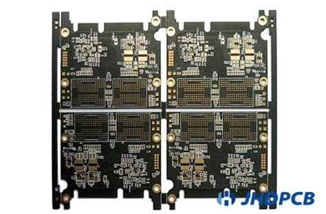
What is PCB Panelization?
PCB panelization is the process of grouping multiple printed circuit board designs onto a single panel for manufacturing. This technique is widely used in the electronics industry to increase production efficiency and reduce costs. By placing several PCBs on a single panel, manufacturers can produce more boards in less time, minimize material waste, and simplify the assembly process.
Benefits of PCB Panelization
- Cost reduction
- Increased production efficiency
- Simplified assembly process
- Minimized material waste
How Does PCB Panelization Work?
The PCB panelization process involves several steps to ensure that the individual boards are correctly arranged on the panel and can be easily separated after manufacturing. Here’s a general overview of the process:
-
Design preparation: The individual PCB designs are reviewed and optimized for panelization. This includes ensuring adequate spacing between boards, adding fiducial marks for alignment, and incorporating any necessary tooling or Breakaway Tabs.
-
Panel layout: The optimized PCB designs are arranged on a single panel layout. The layout takes into account the dimensions of the manufacturing equipment, the required spacing between boards, and any specific requirements for the assembly process.
-
Tooling and breakaway tabs: Tooling holes and breakaway tabs are added to the panel layout. Tooling holes are used to secure the panel during the manufacturing process, while breakaway tabs allow for easy separation of the individual boards after production.
-
Manufacturing: The completed panel layout is sent to the manufacturing facility, where the panels are fabricated using standard PCB production techniques such as etching, drilling, and plating.
-
Depanelization: After the manufacturing process is complete, the individual boards are separated from the panel using the breakaway tabs. This process, known as depanelization, can be done manually or using specialized equipment.
Types of PCB Panelization
There are two main types of PCB panelization: tab routing and v-scoring.
-
Tab routing: In this method, small tabs are left connecting the individual boards to the panel frame. These tabs are later broken off during the depanelization process. Tab routing is a cost-effective option for smaller production runs and less complex designs.
-
V-scoring: V-scoring involves creating shallow grooves along the edges of each individual board. These grooves make it easier to snap the boards apart after manufacturing. V-scoring is preferred for larger production runs and more complex designs, as it provides cleaner breaks and reduces the risk of damage to the boards.

Considerations for PCB Panelization
When planning for PCB panelization, there are several key factors to consider:
-
Board size and shape: The size and shape of the individual boards will determine how they can be arranged on the panel. Irregular shapes or large boards may require special consideration to ensure efficient panelization.
-
Spacing and clearance: Adequate spacing between boards is essential to prevent damage during the manufacturing and depanelization processes. The specific spacing requirements will depend on the chosen panelization method and the capabilities of the manufacturing equipment.
-
Material selection: The choice of PCB material can impact the panelization process. Some materials may be more prone to warping or damage during manufacturing, which can affect the quality of the final product.
-
Assembly requirements: If the PCBs will undergo additional assembly processes, such as component placement or soldering, the panelization layout must take these requirements into account. This may involve adding extra space for Component clearance or incorporating specific tooling features.
-
Cost and production volume: The choice of panelization method and the overall panel layout will be influenced by the desired production volume and budget constraints. Larger production runs may justify more complex panelization techniques, while smaller runs may prioritize cost-effectiveness.

Advantages of Working with Screaming Circuits for PCB Panelization
Screaming Circuits is a leading provider of PCB Assembly services, offering expertise in PCB panelization for projects of all sizes. By working with Screaming Circuits, you can benefit from:
-
Experience and expertise: The team at Screaming Circuits has extensive experience in PCB panelization, ensuring that your designs are optimized for manufacturing efficiency and quality.
-
Customized solutions: Screaming Circuits can work with you to develop a panelization strategy that meets your specific requirements, taking into account factors such as board size, production volume, and assembly needs.
-
Advanced manufacturing capabilities: With state-of-the-art manufacturing equipment and a commitment to quality control, Screaming Circuits can deliver high-quality panelized PCBs for your projects.
-
Rapid turnaround times: Screaming Circuits understands the importance of meeting tight deadlines and offers fast turnaround times for PCB panelization and assembly services.
-
Cost-effective solutions: By optimizing your PCB designs for panelization, Screaming Circuits can help you reduce manufacturing costs and maximize your budget.

Case Studies: Successful PCB Panelization Projects with Screaming Circuits
Case Study 1: Medical Device Manufacturer
A medical device manufacturer approached Screaming Circuits with a challenge: they needed to produce a large volume of complex PCBs for a new product, but their current panelization process was inefficient and costly. Screaming Circuits worked with the manufacturer to redesign their PCB layouts for optimal panelization, incorporating v-scoring and specialized tooling features. As a result, the manufacturer was able to reduce their production time by 30% and decrease their material waste by 20%.
Case Study 2: Automotive Electronics Supplier
An automotive electronics supplier needed to produce a series of PCBs for a new vehicle model, but their designs were too large to fit on standard panel sizes. Screaming Circuits collaborated with the supplier to create a custom panelization solution that maximized the available panel space while ensuring adequate clearance for the assembly process. By optimizing the panel layout, Screaming Circuits helped the supplier reduce their manufacturing costs by 25% and meet their tight production deadlines.
Frequently Asked Questions (FAQ)
-
What is the minimum spacing required between boards for PCB panelization?
The minimum spacing between boards depends on the specific panelization method and the capabilities of the manufacturing equipment. Generally, a minimum spacing of 1-2mm is recommended for tab routing, while v-scoring may require slightly larger spacing. It’s best to consult with your PCB manufacturer to determine the optimal spacing for your project. -
Can PCB panelization be used for both prototype and high-volume production?
Yes, PCB panelization can be used for both prototype and high-volume production. However, the specific panelization strategy may differ depending on the production volume. For smaller prototype runs, a simpler tab routing method may be sufficient, while larger production volumes may require more advanced techniques like v-scoring. -
How does PCB panelization affect the cost of my project?
PCB panelization can help reduce the overall cost of your project by increasing manufacturing efficiency and reducing material waste. By grouping multiple boards on a single panel, you can minimize the time and resources required for production. However, the specific cost savings will depend on factors such as the panelization method, board size, and production volume. -
What file formats are required for PCB panelization?
When submitting your PCB designs for panelization, it’s essential to provide the necessary design files in the appropriate formats. Generally, manufacturers require Gerber files (.gbr) for the individual board designs, along with any additional files such as drill files (.drl) or pick-and-place files (.txt or .csv). It’s best to consult with your PCB manufacturer for their specific file requirements. -
How long does the PCB panelization process take?
The time required for PCB panelization depends on the complexity of the designs, the panelization method, and the manufacturer’s workload. Generally, the panelization process itself can be completed within a few days, but the overall production timeline will depend on factors such as the PCB Fabrication and assembly processes. Screaming Circuits offers rapid turnaround times for PCB panelization and assembly services, with many projects completed within 5-10 business days.
Conclusion
PCB panelization is a critical aspect of the electronics manufacturing process, offering numerous benefits such as cost reduction, increased efficiency, and simplified assembly. By working with an experienced provider like Screaming Circuits, you can ensure that your PCB designs are optimized for panelization, resulting in high-quality, cost-effective solutions for your projects.
Whether you’re a small startup or a large enterprise, Screaming Circuits has the expertise and capabilities to meet your PCB panelization needs. With a focus on customized solutions, advanced manufacturing techniques, and rapid turnaround times, Screaming Circuits is your ideal partner for successful PCB panelization projects.


Leave a Reply