Introduction to PCB Manufacturing
Printed circuit boards (PCBs) are the foundation of modern electronics. PCBs provide the mechanical structure and electrical connections for components in electronic devices. As electronic products become smaller, faster and more complex, the demands on PCBs increase. This has led to innovations in PCB design, materials and manufacturing processes.
PCBs are manufactured in high-tech factories that require substantial investments in equipment, facilities and expertise. This article provides an in-depth look at PCB manufacturing factories including the key processes, equipment, quality control and environmental considerations.
PCB Manufacturing Processes
There are several key processes involved in manufacturing PCBs:
1. Design and Fabrication Data Preparation
The PCB fabrication process begins with the board being designed in CAD or PCBA software. The data generated is converted into formats readable by the manufacturing equipment. This includes gerber files, drill files, netlists, BOMs and assembly drawings. Data verification is critical before manufacturing begins.
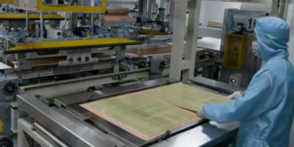
2. Materials Processing
The raw materials for PCBs include laminate sheets made of fiberglass and copper foil. These materials are cleaned, coated and bonded together using heat and pressure to create a board substrate. Holes may be drilled or punched in the board prior to lamination.
3. Imaging and Etching
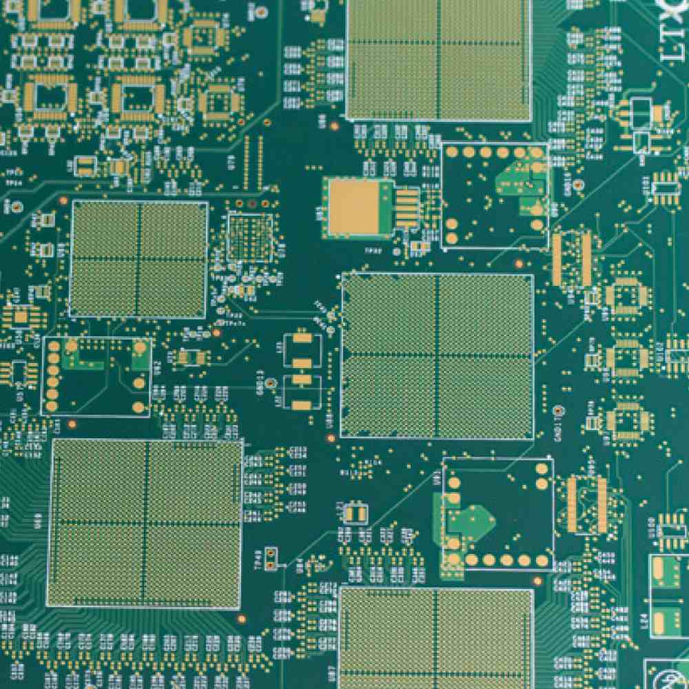
Photoresist is applied to the copper surfaces of the PCB substrate and imaged using ultraviolet light through a photomask. The unexposed photoresist is developed away, leaving a pattern of bare copper. The board is then etched to remove the unwanted copper, leaving only the desired copper circuit pattern.
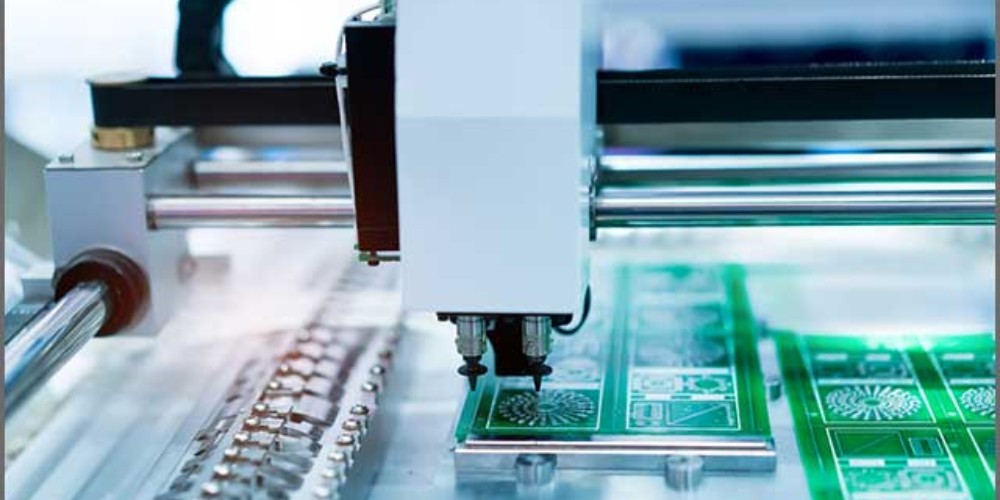
4. Hole Drilling
Holes are drilled in the PCB substrate to allow component leads and vias to pass through. High precision drilling machines create thousands of holes per board. The walls of the holes are plated with copper to provide conductivity.
5. Plating and Coating
The PCBs are electroplated to build up the thickness of the copper circuitry. This is followed by immersion plating of solder, gold or other metallic finishes. Protective coatings such as solder mask and legend ink are applied on the board surfaces.
6. Final Finishing
PCBs undergo a battery of final finishing processes such as routing, depaneling, cleaning, electrical testing and inspection. Automated optical inspection (AOI) systems check for defects. Approved boards are shipped to customers.
PCB Manufacturing Equipment
PCB factories contain an array of advanced manufacturing equipment engineered for high precision and productivity. Here are some of the key equipment types:
- Laminators: Apply high pressures and temperatures to bond sheets of laminate material together. This forms the PCB substrate.
- Imaging Machines: Use UV light to transfer the circuit pattern from photomasks to photoresist on boards.
- Etchers: Selectively remove copper from boards to form the conductors. Common types are wet chemical etchers and plasma etchers.
- Drilling Machines: Drill thousands of tiny holes in boards for component holes and vias. Optimal hole wall roughness and accuracy is critical.
- Plating Equipment: Electroplate copper and other metals onto boards to build up conductor thickness and create metallic finishes.
- Coating/Developing: Apply, expose and develop solder mask, legend ink and other coatings onto boards.
- AOI Systems: Automated optical inspection systems using high resolution cameras to inspect PCBs for defects.
- Testers: Test functionality of PCB electrical connections and identify faults.
Quality Control
Maintaining quality is paramount in PCB production. Printed circuit boards are inspected throughout the manufacturing process:
- Data Quality: Gerber files, drill files and BOMs are rigorously checked before production starts. This prevents errors from propagating through the process.
- In Process Inspection: Boards are inspected after key process steps (imaging, etching, drilling, etc). This catches defects early when corrective action is fastest.
- AOI: Automated optical inspection systems quickly scan boards to identify any small defects or contaminants.
- Electrical Testing: Continuity, shorts and opens are tested on finished boards to verify all connections function properly.
- Outgoing Quality Inspection: Final quality control checks before shipment ensure all customer requirements are met.
Extensive process controls are implemented on equipment, materials and personnel. Statistical process control is used to monitor processes and detect variations. When defects occur, root cause analysis helps identify and correct the source of the problem.
Environmental Considerations
PCB factories require significant energy, water and raw material consumption. Hazardous wastes are generated from metals, acids/alkalis, solvents and more. Managing the environmental impact is crucial.
- Pollution Control: Air emission and wastewater scrubbers remove toxic gases and particulates before discharge. Zero liquid discharge systems recycle water.
- Waste Management: Solid and hazardous wastes are properly stored, treated, recycled and disposed of according to regulations.
- Energy Efficiency: Energy efficient equipment, lighting and HVAC systems minimize electricity usage.
- Materials Conservation: Chemicals, metals and water are recycled and reused to reduce raw material demands.
- Compliance Audits: Regular audits ensure the facility remains in compliance with all environmental regulations. ISO 14001 certification is common.
With rising environmental standards worldwide, PCB factories are prioritizing reducing their ecological footprint through process optimization, new technologies and sustainable best practices.
Key Considerations When Choosing a PCB Manufacturer
Selecting the right PCB manufacturing partner is crucial to getting quality boards delivered on time at a competitive cost. Here are some key factors to evaluate:
- Capabilities: Look for manufacturers with capabilities matching your design needs – number of layers, board sizes, hole sizes, tolerances, finishes, etc.
- Quality Systems: Choose companies that are certified to quality standards like ISO 9001. They should have extensive quality control procedures and traceability.
- Volume Production: Opt for high volume manufacturers if you require regular production runs in the thousands of boards. They will have optimized processes.
- Prototyping: For low volume prototyping needs, find companies experienced in quick-turn prototype services. Check their design for manufacturability feedback.
- Supply Chain: Select manufacturers with established supply chains for materials, equipment and components to avoid potential delays.
- Customer Service: Look for responsive sales and engineering support for a collaborative manufacturing experience. On-time delivery history should be >90%.
- Location: Geographic proximity reduces shipping costs and lead times. However, excellent remote coordination is possible if communication is very good.
- Cost: Get pricing from multiple manufacturers to compare. Look beyond unit costs at total cost considering logistics, quality and inventory management savings from working with a particular supplier.
Finding the best match on these criteria will produce a smooth PCB manufacturing partnership and get your products to market faster.
Frequently Asked Questions
1. What are the different types of PCBs?
The most common types of PCBs are:
- Single sided – conductors on one side only
- Double sided – conductors on both sides
- Multilayer – conductors and insulating layers laminated into a sandwich
- HDI/Microvia – boards with very fine lines, spaces and microvias
- Flex/Rigid-Flex – flexible boards that can bend and fold
- Metal core – boards with a metal core for enhanced thermal performance
2. What file formats are required for PCB fabrication?
The key file formats needed are:
- Gerber files – contain circuit copper layers, solder mask, legend, etc.
- Drill files – specify hole sizes and locations
- Netlist – defines connectivity between pads/traces
- BOM – materials list of components to mount on the assembled board
- Assembly drawings – show component placement on the board
3. What is the typical lead time for PCB manufacturing?
For prototype quantities, the typical lead time is 5-10 days.
For production volumes of thousands of boards, the lead time is generally 4-6 weeks. It includes time for procuring raw materials, scheduling production and shipping.
Lead times can vary significantly between different manufacturers based on their current capacity and backlog.
4. What factors affect the cost of PCB manufacturing?
Some of the key factors affecting PCB cost are:
- Board complexity – number of layers, density, tight tolerances
- Board size and thickness
- Quantity being produced
- Lead time available
- Special processing – HDI, controlled impedance, etc.
- Special materials – RF materials, flex materials, etc.
- Finishes – immersion gold, ENIG, HASL, etc.
- Testing and inspection requirements
- Location of manufacturer – labor costs and shipping
5. How can defects be prevented in PCB production?
Defect prevention requires:
- Thorough data checking before production
- Inspection of raw materials
- Process control and monitoring
- Frequent in-process inspection during fabrication
- Automated optical inspection of every board
- Testing boards electrically after fabrication
- Traceability systems to isolate defects
- Root cause analysis when defects occur
Following robust quality control procedures throughout the process minimizes overall defects.
Conclusion
PCB manufacturing is a complex process requiring significant expertise and capital equipment investments. Understanding the key processes, quality systems, environmental considerations and selection criteria allows for choosing the optimal PCB partner. With attention to detail, continuous improvement and quality control, PCB factories can reliably manufacture boards to support today’s demanding electronics.


Leave a Reply