Introduction
Printed circuit boards (PCBs) are an essential component of most modern electronic devices. They provide the mechanical structure and electrical connections between components to create complex circuits and systems. The manufacturing and assembly of high-quality PCBs is crucial for building reliable, functional electronic products. This guide will examine the key steps and considerations for PCB fabrication and assembly.
PCB Design and Layout
The first stage in creating a new PCB is designing the board layout. This involves using CAD software to map out the placement of components, routing of copper traces between pads, and definition of board layers and stackup. Important factors in PCB layout include:
- Component placement – optimize for efficient routing and minimize wire lengths
- Trace routing – avoid crosstalk and match impedances
- Layer stackup – designate signal, power, ground layers
- Board dimensions – allow space for components and connectors
- Copper weight – balance cost and current capacity
- Test points – include for validation and debugging
The output of PCB layout is a set of Gerber files that define the traces, drill holes, and layers for board fabrication.
PCB Fabrication
PCB fabrication transforms the Gerber files into a physical board. The key steps are:
1. Copper Patterning
The conductive copper layer is coated onto the insulating substrate material through processes like laminating or sputtering. Photoresist is then applied and the Gerber files are used to pattern the copper into the desired trace layout.
2. Etching
Unwanted copper is etched away, leaving only the exposed traces. Common etching methods include chemical etching, plasma etching, and laser direct imaging (LDI).
3. Hole Drilling
Holes are mechanically drilled through the board to connect layers and allow component leads to pass through. The diameter and location is specified by drill files.
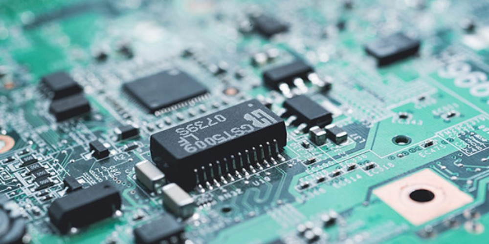
4. Plating and Coating
Connecting traces between layers requires plating the drilled holes with copper. The board then receives coatings like solder mask, silkscreen, and finishes.
5. Electrical Testing
Fabricated boards undergo testing to verify the insulation, continuity, and functionality of the designed circuits.
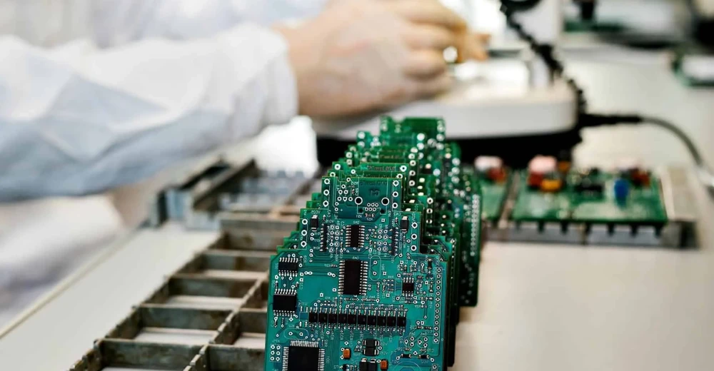
PCB Assembly
Populating fabricated PCBs with components creates a functional board assembly. This involves:
1. Component Preparation
Components like ICs, resistors, and connectors are sourced and prepared with leads or pads for soldering.
2. Solder Paste Application
Solder paste is stenciled or printed onto pads for surface-mount components.
3. Pick and Place
Robotic pick and place machines precisely position components on the board.
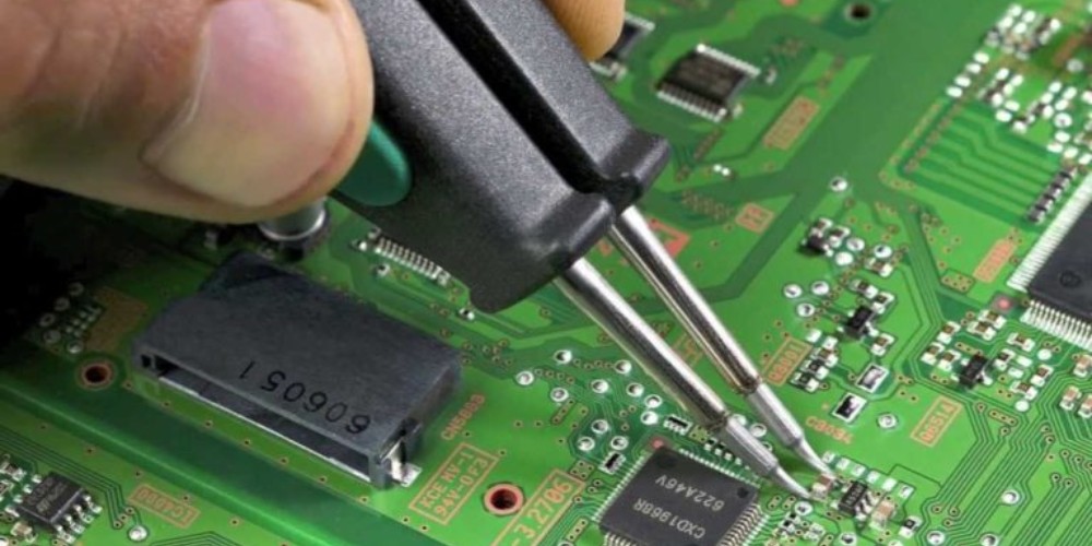
4. Soldering
The boards pass through soldering ovens to melt the solder paste and attach components. Wave soldering can solder through-hole parts.
5. Cleaning and Inspection
Residues are cleaned off and assemblies are visually inspected or x-rayed for defects.
6. Programming and Testing
For programmable devices like microcontrollers, firmware is loaded and functional tests performed.
| PCB Fabrication | PCB Assembly |
|---|---|
| Copper Patterning | Component Preparation |
| Etching | Solder Paste Application |
| Hole Drilling | Pick and Place |
| Plating and Coating | Soldering |
| Electrical Testing | Cleaning and Inspection |
| Programming and Testing |
Choosing A PCB Manufacturer
Key factors in selecting a PCB manufacturing partner:
- Capabilities – evaluate available substrates, layer counts, tolerances
- Quality – review process controls, certifications, failure rates
- Lead Times – assess scheduling flexibility, rush services
- Cost – compare pricing models and volume discounts
- Supply Chain – ensure component availability for assembly
- Customer Service – test response time and problem resolution
Leading global PCB manufacturers include Jabil, Flex, Benchmark Electronics, and Sanmina.
Conclusion
Successfully designing, fabricating, and assembling PCBs requires attention to details at each step. Planning board layouts for manufacturability and partnering with a capable manufacturer optimizes quality, cost, and time-to-market for electronic products. Following best practices in PCB development enables creating smaller, faster, and more reliable circuits.
Frequently Asked Questions
What are some key considerations in PCB component placement?
Some key factors in component placement are: minimizing wire lengths, grouping related circuits together, allowing space for routing between parts, keeping high-speed traces short, and placing heat-sensitive ICs away from hot components.
How accurate is PCB hole drilling?
Modern mechanical drilling can achieve very high accuracies, with tolerances down to +/- 0.002 inches for hole size and +/- 0.005 inches for hole position. Laser direct imaging allows even finer resolution down to +/- 0.001 inches.
What types of coatings are applied to PCBs?
Common PCB coatings include solder mask to prevent solder bridging, silkscreen for component legends, and finishes like HASL, immersion tin, or ENIG to protect copper traces. Conformal coatings can be applied to provide environmental protection.
How are surface mount components held in place before soldering?
Solder paste applied to the PCB pads helps hold components. Some passive parts may use adhesives. Larger BGAs and connectors may have temporary fasteners for alignment. The pick and place process precisely positions parts.
What testing is performed on assembled PCBs?
Testing will include inspection of solder joints with x-ray, testing power and signals, programming firmware, functional test of assemblies, and environmental stress screening through temperature cycling and vibration.


Leave a Reply