Introduction to PCBs
A printed circuit board (PCB) is a laminated board made of non-conductive substrate material with conductive pathways etched from copper sheets and laminated onto the substrate. PCBs allow electrical components like resistors, capacitors, integrated circuits, and others to be mechanically supported and electrically connected using conductive tracks, pads, and other features etched from copper sheets and onto the substrate.
PCBs provide the foundation for almost all modern electronics, from simple devices like calculators to complex computer systems and machinery. Understanding the PCB manufacturing process is key for engineers and designers looking to produce functional, high-quality boards.
This comprehensive guide will walk through the typical PCB production workflow – from designing the board layout to assembling the final product.
The PCB Design and Layout Stage
The first step in manufacturing a custom PCB is designing the board itself. This involves:
Schematic Capture
This is the process of drawing a schematic diagram to represent the logical connections between electrical components on the board. Symbols are used to depict the components while lines show their electrical connections. Schematic capture is usually done using CAD software tools.
PCB Layout
Once the schematic is completed, the PCB layout can be designed. This involves mapping out the physical locations of components, routing tracks to electrically connect them, defining board dimensions, adding mounting holes, etc. PCB layout software allows engineers to design boards efficiently.
Design Rule Checks
Design rules specify constraints like minimum spacing between tracks, allowable trace widths, and more. CAD tools run design rule checks (DRCs) to ensure the PCB layout adheres to these rules. This prevents electrical shorts, improper clearances, and other issues.
Simulation and Analysis
Engineers can simulate circuit behavior, signal integrity, thermal performance, and other parameters during the design process itself to verify the board’s functionality before manufacturing. Tools like waveform viewers, signal integrity analyzers, and thermal modeling aid in analysis.
Outputting Design Files

Once the board layout is finalized, the PCB design software generates output files used for fabrication and assembly. Key file formats include:
- Gerber Files: Contains circuit board layers, drill holes, copper layers, solder mask layers, legend or silkscreen layers, etc. There are separate Gerber files for each layer/section.
- Drill Files: Specifies information on all the holes to be drilled in the PCB including their locations and sizes.
- Bill of Materials (BOM): Lists all the components used in the circuit along with information like reference designators, values, quantities, etc.
- Assembly Drawings: Illustrates component locations, orientations, and part numbers as a reference for PCB assembly.
- Netlist: Lists all the electrical connections between components.
These files are essential for the PCB fabrication and assembly process downstream.
Choosing a PCB Manufacturer
With the design files in hand, the next step is selecting a suitable PCB manufacturing partner who can produce the boards reliably at a reasonable cost. Key factors in choosing a PCB manufacturer include:
- Capabilities: The manufacturer should be able to offer all necessary PCB fabrication processes – from imaging to final testing. This includes services like solder mask, silkscreen, surface finishes, controlled impedance, HDI, etc.
- Quality: They should have robust quality assurance procedures and test methods at various stages of production. Certifications like ISO 9001 are a plus.
- Volume Capabilities: The vendor should be capable of supporting low to high volume production runs as needed.
- Lead Times: Acceptable turnaround times for both prototypes and production quantities. Faster lead times allow for quicker product development.
- Location: Vendors located close to the designer/engineer allow for better communication and logistics. However, overseas manufacturing can offer significant cost savings.
- Cost: Affordable pricing for required order quantities without compromising quality. Get quotes from multiple manufacturers.
The PCB Fabrication Process
Once a PCB manufacturer is selected, the fabrication process begins. Here are the typical stages involved in transforming design files into finished boards:
1. Submitting Design Files
The Gerber, drill, netlist, and other files are submitted to the manufacturer. CAM engineers check the files thoroughly.
2. Film Processing
The PCB image is printed onto an oversized photographic film using a high precision imagesetter machine. This film acts as a photomask for the next steps.
3. Board Material Preparation
The base laminate PCB substrate is cut to size and drilled for any holes. This preprocessed board panel gets cleaned and prepared.
4. Photoresist Lamination
A layer of photoresist is applied on the board surface. Photoresist is a light-sensitive polymer that forms a coating on the substrate.
5. Imaging/Exposure
The photoresist-coated board is aligned with the film photomask produced earlier. UV light is used to transfer the PCB image onto the photoresist.
6. Developing
The board is treated with a chemical developer. This removes the unexposed photoresist while the UV exposed areas remain intact. This leaves a patterned photoresist layer on the substrate.
7. Etching
Etchant chemicals like ferric chloride dissolve away the exposed copper regions that are unprotected by photoresist. This leaves only the desired copper circuit pattern on the PCB.
8. Photoresist Stripping
Any remaining photoresist is now removed from the board using a different chemical. This leaves behind just the copper circuitry pattern.
9. Surface Finishing
The fabricated boards are put through a variety of finishing processes like soldermask coating, silkscreen printing, surface plating, etc.
10. Electrical Testing
Finished boards undergo comprehensive electrical tests. Any boards failing tests are discarded.
11. Quality Inspection
Sample testing and visual inspection at multiple points in the process ensure consistent quality.
12. Panel Singulation
The large fabricated board panels are cut into individual PCBs. The boards are packed and shipped to the customer.
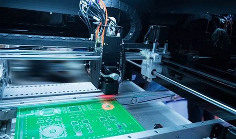
Assembling Components onto PCBs.
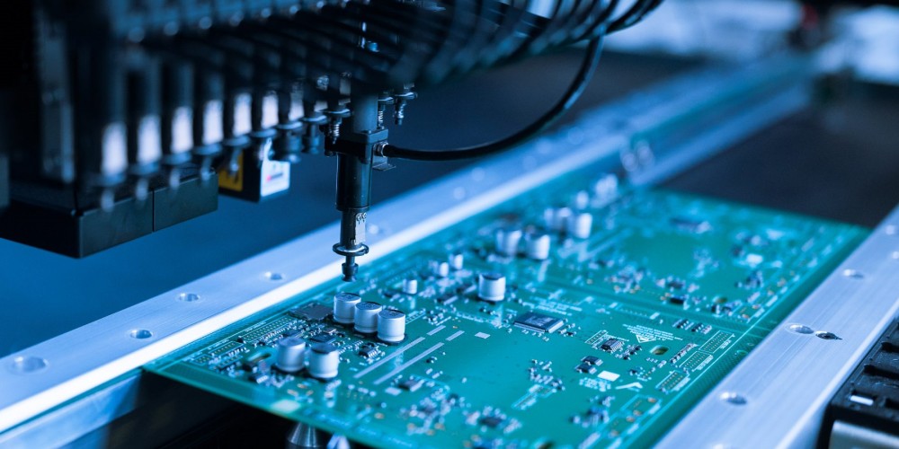
The bare fabricated PCBs must now be populated with the required electronic components to form a functional printed circuit assembly (PCA). This is done using two methods:
1. Through-Hole Assembly
Components with wire leads are inserted into holes in the PCB and soldered from the opposite side to form mechanical and electrical connections. Wave soldering machines automate through-hole assembly.
2. Surface-Mount Assembly
SMD (surface-mount device) components are placed onto contact pads on the PCB surface. Reflow soldering melts solder paste to form solder joints to attach components. Pick-and-place machines enable automated assembly.
Other assembly processes like conformal coating, programming, testing, etc. may be required to complete PCA manufacturing.
Comparison of Through-Hole and SMD Assembly:
| Assembly Method | Description | Pros | Cons |
|---|---|---|---|
| Through-hole | Leaded components inserted into plated holes | Simple process<br>Easily soldered and desoldered | Low component density<br>Manual labor intensive |
| Surface-mount | Components soldered directly onto surface pads | Higher density<br>Automated assembly | More complex soldering process |
Conclusion
Manufacturing PCBs involves many steps – from precise board layout using CAD software to photolithographic fabrication techniques and component assembly processes. Advancements continue to enable more complex board designs with shrinking feature sizes, multiple layers, and rigorous quality requirements. By selecting an experienced PCB manufacturer and providing comprehensive design files, engineers can receive cost-effective and high-performing printed circuit boards in their electronic products.
Frequently Asked Questions
What are the different types of PCB substrate materials used?
Some common PCB substrate materials include:
- FR-4 – Flame retardant woven fiberglass with an epoxy resin binder. The most popular and cost-effective option.
- CEM-1 – Cotton paper and epoxy composite material. Low cost but lower performance than FR-4.
- PTFE – Polytetrafluoroethylene based high-frequency boards with excellent electrical insulation.
- Polyimide – Flexible boards that can withstand high temperatures. Used for flexible circuits.
- Aluminum – Metal core PCBs for high thermal conductivity.
What are the advantages of using a 4-layer PCB vs 2-layer?
4 layer PCBs offer better noise isolation, higher component density, improved power distribution, and extra space for routing complex designs. The inner layers also act as a thermal heatsink. However, 4-layer boards have higher fabrication costs than simpler 2-layer boards.
Should PCB traces be designed on a grid?
Using a routing grid makes PCB layout faster and more efficient. Components and vias can be aligned on grid intervals instead of arbitrary placements. A grid minimizes trace lengths and via counts. Grid-based layouts are easier to edit with CAD tools.
How are very dense PCB designs with tiny features manufactured?
High density interconnect (HDI) technology allows packing more features into a given PCB area. This includes thinner trace widths and spaces below 5 mils, microvias under 6 mils, and more. HDI uses newer fabrication processes like laser drilling and advanced materials to enable multilayer boards with over 20 layers if needed.
What safety precautions should be taken when handling PCBs?
- Avoid touching exposed solder joints and component leads to prevent electrostatic discharge damage. Use ESD-safe gloves and mats.
- Wash hands after handling PCBs to prevent any chemical exposure from solder or flux residue.
- Wear safety goggles when desoldering or modifying boards to prevent eye injuries.
- Ensure adequate ventilation when soldering. Use fume extractors to remove solder flux fumes.


Leave a Reply