Introduction
Printed circuit boards (PCBs) are an integral part of almost every electronic device we use today. From smartphones and laptops to industrial equipment and medical devices, PCBs provide the foundation for mounting and connecting electronic components using conductive tracks and pads.
The process of taking a PCB design from concept to finished board is known as PCB fabrication and assembly. In this comprehensive guide, we will look at every step involved in prototyping and manufacturing PCBs, from the design stage through to assembly and testing.
PCB Design
The first step in the PCB production process is creating the board layout. This is done using CAD (computer-aided design) software such as Altium, Eagle, or KiCad. The PCB designer will create schematics showing connections between components and then design the board outline and layout based on circuit requirements and manufacturing guidelines.
Several key factors need to be considered during PCB design:
- Component placement – Parts must be arranged logically taking into account signal paths, heat dissipation, access for testing, and other factors. CAD tools help optimize placement.
- Trace routing – This involves connecting component pins and pads with copper tracks on different layers. Constraints include track width, spacing, length matching, and impedance control.
- Board layers – Multi-layer boards allow more complex, denser designs. Typical layer counts are 2 to 12 or more.
- Via pads – Pads for vias that interconnect layers must be allowed for. Certain rules govern their size and spacing.
- Board outlines – The dimensions and shape of the PCB must be planned with manufacturing and assembly in mind.
- Fabrication data – The CAD tool outputs files such as Gerber and drill data to guide PCB fabrication.
| PCB Design Stage | Details |
|---|---|
| Schematics | Shows electronic connections |
| Component placement | Arrange parts for routing, thermal needs, etc |
| Trace routing | Connect components with tracks on layers |
| Layer stackup | Choose number of copper layers |
| Via design | Plan pads for vertical interconnects |
| Board outline | Design board dimensions and shape |
| Manufacturing outputs | Gerber files, drill data, etc |
Prototyping vs Production
Once the PCB layout is complete, the designer must decide whether to produce prototypes first or go directly to full production.
Prototyping involves making a small number of boards (typically 5-10) to test the design before manufacturing a full batch. This verifies the design is functional and catches any errors early.
Production means manufacturing a larger quantity of boards (anywhere from tens to thousands) for end products. The boards are assembled in volume.
Here is a comparison between prototyping and production:
| Factor | Prototyping | Production |
|---|---|---|
| Quantity | 5-10 boards | Dozens to thousands |
| Lead time | 1-5 days | 15-20 days minimum |
| Cost per board | Higher | Lower due to scale |
| Fabrication process | Similar | Fine-tuned for volume |
| Testing | Design validation | Quality assurance |
| Assembly | Often manual | Automated pick-and-place |
| Applications | Proof of concept | End products |
In most cases, it’s advisable to first prototype a small batch to de-risk the design before investing in volume production.
PCB Fabrication Process
PCB fabrication involves taking the design files from CAD and physically manufacturing the bare circuit boards. This is done at specialized PCB manufacturing facilities.
Here are the key steps in fabricating prototype and production PCBs:
1. Import Design Files
The Gerber, drill, and other CAD-generated files are imported into the PCB manufacturer’s CAM (computer-aided manufacturing) software. The data is checked for errors.
2. Create Fabrication Data
The CAM software combines the design layers and generates detailed instructions for the PCB fabrication equipment.
3. Select Base Material
The type of circuit board material depends on requirements like number of layers, frequency, thermal needs, and cost. Typical materials are FR-4 glass epoxy and high-frequency RF materials.
4. Clean and Coat Panels
Sheets of the PCB substrate are cleaned and coated with photoresist, a photosensitive chemical.
5. Image Inner Layers
For multilayer boards, artwork patterns for the inner layers are optically transferred onto the coated sheets.
6. Etch Inner Layers
The unexposed photoresist is washed away, leaving only the desired copper traces. The sheets are then etched to remove copper from unmasked areas.
7. Laminate Board Stack
Sheets are stacked together along with pre-preg bonding material and laminated under heat and pressure to form a multilayer board.
8. Drill Holes
Holes are drilled for vias that interconnect layers and for component mounting. Excellent drill-to-hole alignment is critical.
9. Metallize Holes
The boards are electroplated to coat the drilled holes with copper, creating vias and plated through-holes (PTHs).
10. Pattern Outer Layers
Photoresist is applied on outer layers and artwork patterns are transferred. Unexposed areas are etched away.
11. Coat Surfaces
A solder mask is applied to coat the entire board except solderable areas like pads. Silkscreen prints visible markings.
12. Trim and Inspect
Boards are separated from the panel and inspected for defects using automated optical inspection (AOI).
This fabrication process results in finished bare PCBs ready for electronics assembly.
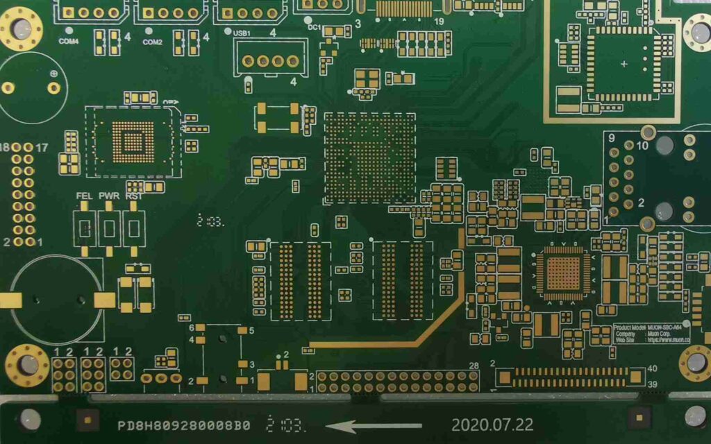
PCB Assembly
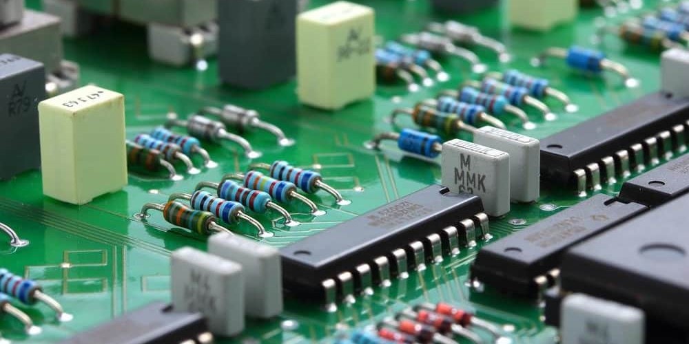
After the bare boards are fabricated, electronic components must be mounted and soldered to assemble a functional printed circuit board. This is called PCBA or PCB assembly.
Here are the steps involved in assembling PCBs:
1. Bill of Materials
All the components required for assembly are listed in a BOM, along with reference designators, quantities, and specifications.
2. Parts Procurement
Components are sourced from various suppliers based on the BOM and procurement plan. Digikey, Mouser, Newark, and Arrow are common sources.
3. Solder Paste Stencil
A thin metal stencil is laser cut with apertures matching the PCB footprint. It is used to apply solder paste on pads.
4. Solder Paste Printing
The stencil is aligned over the PCB and solder paste is applied on pads through the apertures.
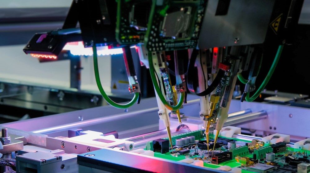
5. Pick-and-Place
Robotic pick-and-place machines rapidly populate boards with components from reels and sticks.
6. Reflow Soldering
Boards pass through a reflow oven heating the solder paste to form reliable solder joints.
7. Cleaning/Coating
Excess flux is cleaned off and a conformal coating may be applied for protection against moisture and contamination.
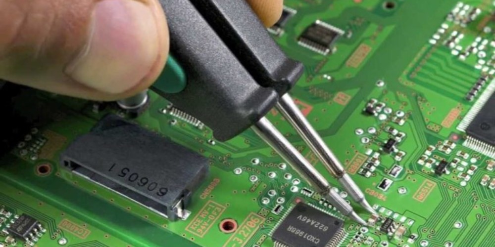
8. Programming/Testing
For programmable boards like microcontroller boards, firmware is loaded and functional tests performed.
This completes the PCB assembly process. The assembled boards can then be integrated into electronic products.
Choosing a PCB Manufacturing Partner
With the basics of PCB fabrication and assembly understood, one of the most important decisions is choosing the right manufacturing partner to produce your boards. Here are some key factors to look for:
- Capabilities – Look for expertise in the services you need – PCB fabrication, component sourcing, soldering, testing, etc.
- Quality – Seek out proven processes for consistent, high-yield manufacturing. Ask about certifications.
- Volume scalability – Partner should have capacity to scale from prototypes to volume production.
- Communication – Ensure clear channels for design reviews, production updates, and technical support.
- Data security – Vet measures taken to protect your valuable IP and design data.
- Cost – Compare pricing models. Seek a balance of cost and capabilities.
- Turnaround time – Ask about lead times for rigid and flex PCB production and assembly.
- Location – Factor in benefits and challenges of domestic or overseas manufacturing.
By selecting the right PCB production partner, you can effectively go from initial concept through prototyping to full-scale production and product release.
PCB Manufacturing Cost Drivers
When budgeting for your PCB project, it helps to understand the key factors that contribute to fabrication and assembly costs. The main drivers are:
- Board size – Generally priced per square inch. Larger boards cost more.
- Layer count – Each layer adds material and process costs. 4-6 layers are common.
- Fine features – High density designs with smaller lines/spaces and via pads cost more.
- Special materials – FR-4 is standard. High-frequency, thermal, and flexible materials are pricier.
- Coatings and finishes – Additional coatings like HASL lead to higher cost.
- Hole count/density – More drilled holes means slower, more precise drilling.
- Tolerances – Tighter tolerances require more process controls.
- Lead times – Faster turnaround times can command a premium price.
- Order volume – Unit price drops significantly at production volumes.
- Assembly – Component sourcing, placement, soldering all impact cost.
- Testing – More rigorous testing like ICT adds cost.
Understanding what drives PCB costs helps you make design decisions upfront and budget realistically.
Factors in High-Quality PCB Manufacturing
Many factors influence the fabrication quality of printed circuit boards. Here are some key aspects manufacturers control to produce top-notch PCBs:
- Material quality – Consistent, high-performance base materials from reputed suppliers.
- Surface finish – Right surface plating like HASL, immersion silver, or ENIG.
- Etching process – Dimensionally accurate photolithographic patterning of copper traces.
- Registration – Precise alignment of artwork layers for electrical connectivity.
- Lamination – No voids, resin starvation, or inconsistencies in multilayers.
- Drilling – High precision CNC drilling with tolerance of +/- 0.002 mm.
- Plating – Uniform copper plating of via holes with 100% throw power.
- Solder mask – Defect-free application with accurate openings for pads.
- Legend printing – Legible reference designators, logos, and text.
- Singulation – Clean cutting without stresses using routers or scoring.
- Inspection – Automated optical and x-ray inspection to catch defects early.
Manufacturers that excel in these areas produce PCBs with maximum yield, reliability long-term reliability in the field.
PCB Design for Manufacturing Guidelines
While designing a PCB, keeping manufacturing best practices in mind ensures your board can be fabricated without issues and functions reliably. Here are some key PCB design for manufacturing (DFM) guidelines:
Trace Width/Spacing
- Minimum trace width and spacing is driven by fabrication capabilities. 0.006″ width/space is typical for 2-layer boards.
- Match trace widths to current levels for optimum performance. Wider traces where high current flows.
- Maintain at least 0.2mm gaps between adjacent traces for consistency in etching.
Copper and Hole Sizes
- Minimum finished hole size is typically 0.2mm. Allow 0.1mm annular ring around holes.
- For inner layers, allow sufficient copper widths around blind/buried vias for plating thickness.
- Follow manufacturer’s via/hole aspect ratio limits based on drill bit lengths.
Solder Mask Expansions
- Provide solder mask clearance of at least 0.1mm around pads and traces.
- Larger expansion on outer layers helps avoid mask bleed during coating.
Text and Logos
- Minimum text height is typically 0.7mm. Allow proper clearances around text areas.
- Use thicker lines and pads under overlaid logos for etching consistency.
Panel Utilization
- Align board outlines efficiently on the fabrication panel to minimize waste.
- Allow sufficient tooling rails between boards for support during fabrication.
Test Points
- Include labeled testpoints to simplify validation and troubleshooting of assembled boards.
Board Outline and Edges
- Include fiducials near board edges for alignment during fabrication and assembly.
- Allow 0.125mm radius on board corners to reduce stress. Avoid sharp corners.
- Bevel board edges slightly (30 degrees) to prevent chipping.
By following DFM principles, PCB designers can help ensure a manufacturable design. This results in short fabrication times, minimal costs, and reliable functioning boards.
New Technologies in PCB Manufacturing
PCB fabrication and assembly continues to evolve with new technologies emerging. Here are some of the advances transforming PCB manufacturing:
HDI PCBs
High density interconnect (HDI) PCBs have finer lines and spaces, smaller vias, tighter tolerances, and higher component density. They allow more routing layers in a thinner board profile. Laser drilling and microvias help achieve the high precision required.
Rigid-Flex PCBs
These combine rigid sections and flexible circuits in one board. Flexible layers interconnect separate rigid areas containing components. This enables products like foldable mobile devices.
Embedded Components
Components are embedded within the PCB layers rather than mounted on the surface. This provides improved electrical performance and heat dissipation while shrinking product size.
Laser Direct Imaging (LDI)
LDI replaces older lamp-based methods for imaging photoresist on PCB layers. Lasers provide higher resolution and precision drilling and routing of PCBs.
Additive Processing
Rather than etching away unwanted copper, additive processes build up traces using plating resists and selective gold/copper plating to reduce waste.
Automation
Integration of automation, data exchange, and analytics is driving improvements across all PCB production processes resulting in higher yields and lower costs.
Conclusion
As PCBs become smaller, denser, and more advanced to power the latest electronic devices, the fabrication and assembly processes must evolve in tandem. Understanding the steps involved helps designers, engineers, and procurement managers implement the best practices to produce innovative, high-quality PCBs in a cost-effective manner. Finding the right manufacturing partner is key to navigating from prototyping to volume production.
Frequently Asked Questions
What are the different types of PCBs based on number of layers?
The four main types of PCBs classified by layer count are:
- Single layer – Copper traces on one side only
- Double layer – Copper on both top and bottom layers
- Multilayer – 4 layers, 6 layers, etc with traces on multiple inner layers
- HDI – High Density Interconnect with microvias and higher layer counts
What design software tools are used for PCB design and layout?
Some popular PCB design software packages are Altium Designer, Cadence Allegro and OrCAD, Mentor Graphics Xpedition, and Autodesk EAGLE. Many offer free versions with limited capabilities.
How long does PCB fabrication and assembly take?
A typical timeframe from completing design to receiving assembled boards is:
- PCB prototyping: 1-5 days
- Small batch PCB production: 10-15 days
- Mass production: 15-25 days
Lead times vary by manufacturer based on order volume and current workloads.
What are the different PCB substrate materials and their applications?
Common PCB substrate materials include:
- FR-4 – Fiberglass-reinforced epoxy laminate, low cost.
- CEM-1 – Cotton paper and epoxy, cost-effective.
- Polyimide – Flexible material for bendable circuits.
- PTFE – Polytetrafluoroethylene for microwave PCBs.
- Ceramic – Alumina or aluminum nitride, high performance, costly.
What tests are performed to ensure quality of fabricated PCBs?
Typical quality tests done by PCB manufacturers include:
- Visual inspection – Check for defects and measurements
- Net connectivity – Validates electrical connections
- ICT – Tests shorts and opens
- Flying probe – Tests continuity between nodes
- AOI – Automated optical inspection of solder mask, legends, etc.
- X-ray – Checks for potential buried defects like voids


Leave a Reply