Overview of PCB Fabrication
Printed circuit boards (PCBs) serve as the foundation for almost all modern electronics. PCBs provide the mechanical structure and electrical connections between components in an electronic device. The fabrication of PCBs involves complex processes to transform raw materials into the multilayer boards that make up electronic circuits. In this comprehensive guide, we will explore the step-by-step manufacturing process behind professional PCB production.
PCB Design and Layout
The first stage in PCB fabrication is the design and layout of the board itself. PCB design is generally done with Electronic Design Automation (EDA) software such as Altium, Cadence, or KiCad. The designer creates schematics showing the electronic connections between components. The schematic is then translated into a physical layout showing the placement of components and tracing of copper tracks on the PCB layers.
Key aspects of the design process include:
- Schematic capture and simulation
- Board outline and layer stack planning
- Component placement and routing
- Design rule checking
- Manufacturing output generation
The output of the PCB layout stage is a set of manufacturing files – usually Gerber files and drill files. These files precisely specify the location of copper tracks, solder pads, and holes to mill in the finished board.
Prototyping vs Production
There are two main categories of PCB fabrication:
Prototyping
Prototyping produces small quantities of boards – usually just a handful. This allows engineers to test new designs and make iterations during development. Prototyping services typically offer faster turnaround but higher costs per board. Popular techniques include:
- Milling/routing from rigid laminate boards
- Laser direct imaging of photoresist
- CNC drilling
Production
Production PCB fabrication generates boards at scale – anything from tens to millions of boards. Production processes leverage specialized equipment to optimize quality, throughput, and cost. Mass production techniques include:
- Photolithography for etching tracks
- Plating for conductive layers
- Lamination for multilayer boards
- Automated assembly
This guide will focus primarily on the production-scale PCB fabrication process.
PCB Base Materials
PCBs start with an insulating substrate material. The most common modern PCB material is FR-4 fiberglass epoxy laminate. Alternatives include ceramics, Teflon, and flexible substrates like polyimide. Key properties include:
- Dielectric constant – Impacts signal speed and crosstalk
- Loss tangent – Losses that degrade high frequency signals
- Thermal conductivity – Ability to dissipate heat from components
- CTE – Coefficient of thermal expansion affects thermomechanical reliability
- Tg – Glass transition temperature should exceed soldering temps
The substrate provides mechanical support and forms the foundation for building up the conductive copper layers.
Inner Layer Processing
The core of multilayer PCBs is built up first by processing the inner layers:
1. Copper Foil Lamination
Sheets of copper foil are laminated onto both sides of the PCB substrate using heat and adhesive. Common foils are 1/2 to 2 oz thickness (0.5-2 mil). Rolls of foil and substrate are fed through a continuous lamination machine.
2. Photolithography
A photosensitive dry film is applied on top of the copper foils. Next, a phototool containing the layer image is used to selectively expose the dry film. Exposed areas are hardened while unexposed areas stay soluble.
3. Developing and Etching
The board is developing in solvents to remove the soluble photoresist and expose the intended copper pattern. Etching chemicals are then used to eat away unwanted copper, leaving only the desired copper traces on the substrate.
4. Photoresist Stripping
After etching, the remaining photoresist is stripped away using a chemical stripper, leaving behind just the copper layer pattern.
5. Repeat For Number of Layers
The photolithography process is repeated for each layer of circuitry in the PCB stackup. Connections between layers are made with plated through holes (PTHs) or vias.
Outer Layer Processing
Once the multilayer core is complete, processing shifts to the outer layers:
1. Layup
The multilayer core is interleaved with additional copper clad substrates using adhesive. This adds extra rigidity and allows circuitry on the outer surfaces.
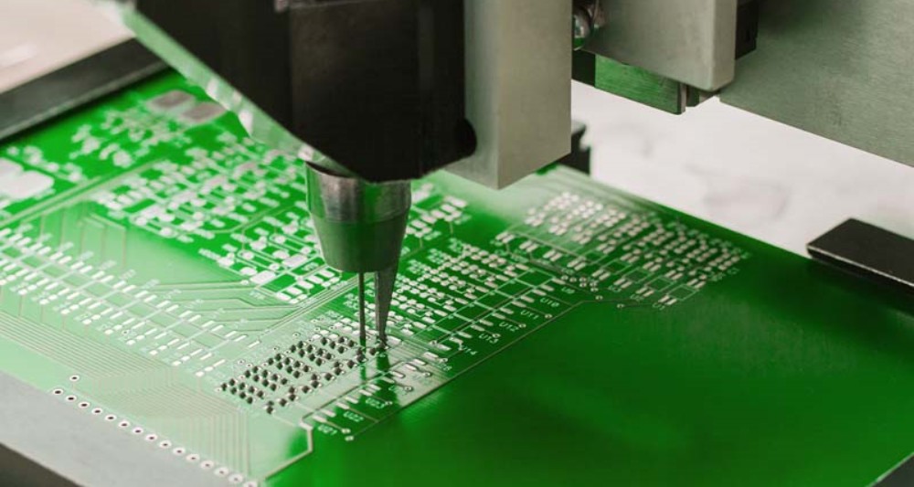
2. Drilling
A CNC drill creates the network of holes that connect layers vertically. High throughput machines can drill over 100,000 holes per hour.
3. Plating
The boards are put through an electroplating bath to coat the drilled holes with a thin layer of copper. This forms a conductive interconnection between layers.
4. Outer Layer Photolithography
The outer layer copper goes through the same photolithographic patterning process as the inner layers to form the external wiring.
Solder Mask and Silkscreen
After etching the outer layers, two additional coatings are applied:
- Solder mask is a polymer layer that functions as solder resist – preventing bridges between pads during assembly. It is green in color.
- Silkscreen applies identifying text, symbols, and markings using epoxy ink. It helps locate components and features during assembly.
Both coatings are printed using lithographic processes.
Final Finishing
The last steps transform the PCB panels into finished boards:
- Routing splits apart individual boards from the large panel.
- Corner chamfering and bevelling smoothes board edges.
- Deburring removes rough copper edges from drilling.
- Testing validates PCB functionality and specs.
- Population can add connectors or components.
Finished PCBs are then shipped to customers for installation of components and devices.
Benefits of Using a PCB Manufacturer
While it’s possible to etch your own boards at home, professional PCB production offers many advantages:
- Economies of scale – Dramatically lower costs per board
- Precision – 0.1 mm traces and 0.15 mm drill holes
- Reliability – Stringent quality control results in very low defect rates
- Turnaround time – As fast as 24 hours from order to delivery
- Scalability – Ability to manufacture tens to millions of boards
- Expertise – Material selection, DFM, and complex fabrication processes
Using an experienced PCB manufacturer like PCBCart ensures high-quality boards with fast turnaround at competitive prices. Their online quoting tools make ordering prototyping and production runs simple.
Frequently Asked Questions
What are the typical lead times for PCB fabrication?
For prototyping services, lead times can be as fast as 24 hours for simple boards. More complex designs are typically 3-4 days. For production PCB runs, standard lead times range from 3-10 business days.
How are multilayer boards held together?
Multilayer PCBs use sheets of prepreg resin to bond together layers under heat and pressure. The resin flows and cures to form a strong composite structure.
What is HDI technology?
High density interconnect (HDI) allows routing traces and spaces under 100 microns to increase circuit density. It enables tighter component spacing and more I/O connections.
Can PCBs be repaired if damaged?
Minor damage can often be repaired. More significant damage usually requires complete replacement of the PCB. It is not economical to repair multilayer boards.
What are common PCB defects?
Typical defects include shorts, open traces, pinholes, clearance violations, annular ring inconsistencies, and non-conformances of finished board dimensions.
Conclusion
PCB fabrication leverages sophisticated processes and specialized equipment to produce quality printed circuit boards. Following the PCB design and layout, inner layers are created using print-and-etch techniques. Multilayer cores then have outer circuit layers added. Additional coating, drilling, and finishing complete the boards. Using a professional PCB manufacturer can ensure reliable, high-performance PCBs tailored to your project needs.


Leave a Reply