Printed circuit boards (PCBs) are an essential component of modern electronics. A well-designed PCB makes manufacturing efficient, reduces costs, and improves product quality and reliability. Here are some key considerations when designing PCBs for manufacturing.
Component Placement
Strategic component placement is crucial in PCB design. Follow these guidelines:
- Prioritize components. Place critical, heat-sensitive, and high-pin-count components first.
- Group similar components. Group all capacitors together, resistors together, etc. This simplifies PCB assembly.
- Observe clearance rules. Leave ample clearance around components for soldering and rework.
- Allow for thermal considerations. Leave space between high-power components to avoid overheating.
- Optimize for efficient routing. Place components to minimize track lengths and complexity.
- Standardize placement where possible. Consistent, standardized component placement makes assembly easier.
Board Size
Keep the PCB compact, but allow room for components and spacing rules:
- Minimize board size. Smaller boards use less material and cost less. But don’t sacrifice usability and clearance rules.
- Standardize board sizes where possible. Standard sizes leverage economies of scale in manufacturing.
- Allow room for connectors and hardware. Account for external connections like cables and enclosures.
- Consider panelization. Manufacturing panels utilize board space efficiently for bulk production.
Component Selection
Component selection directly impacts manufacturability:
- Prefer surface mount devices (SMD). SMDs allow higher density and lower costs than through-hole components.
- Minimize component count. Fewer unique components means simpler sourcing and assembly.
- Select common component sizes. Standard 0603 or 0805 sizes are easiest to work with. Avoid very small or large packages.
- Consider lead-free components. Lead-free parts meet environmental regulations in many regions.
- Choose readily available components. Standard, commonly-used parts are easy to source.
- Define any critical components upfront. Some parts can have long lead times or go obsolete.
Layer Stackup
A properly designed layer stackup optimizes manufacturability and cost:
- Minimize layer count if possible. 2 layer boards are cheapest, with 4-6 layers typical for more complex designs.
- Allocate functions by layer. Use top and bottom layers for high-speed signals. Put power and ground planes in the middle.
- Use thicker copper weights for power planes. 2oz or 3oz copper in power layers reduces resistance and heating.
- Include a soldermask layer. Soldermask insulates copper traces and prevents solder bridges.
- Consider a silkscreen layer. Silkscreen aids visual inspection and debug by printing reference designators.
- Specify board finish. Common finishes are HASL, Immersion Silver, ENIG, and OSP.
Routing and Traces
Proper trace routing improves performance and manufacturability:
- Use appropriate trace widths. 0.2-0.3mm tracks for signals, wider tracks for power. Follow spec sheet limits.
- Observe clearance rules between traces. 0.2mm clearance is typical between signal layers. More for voltage differences.
- Use 45° and 90° angles. Avoid acute angles, curves, and arcs. These are harder to manufacture.
- Avoid trace length mismatches in differential pairs. Matched lengths minimize skew between differential signals.
- Minimize the number of vias. Lots of drilled vias increase cost and reduce reliability.
- Space vias appropriately. 0.3-0.5mm clearance between vias; more for high-power vias.
Silkscreen and Text
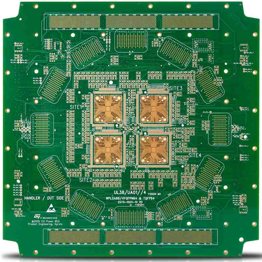
Silkscreen and text aids in visual checks during assembly and debug:
- Add reference designators. Print part reference labels like R1, U3, C5 for easy identification.
- Include polarity indicators. Show polarity markers (+/- symbols) for diodes, caps, and connectors.
- Add useful text legends. Board name, revision, copyright notices, etc help with identification.
- Print outlines of components or connectors. Visual outlines improve alignment during assembly.
- Orient text to be readable. Print text parallel to board edges, not at odd angles. Right-reading for assemblers.
- Use large text sizes. At least 10 point text, bigger for critical markings. Small text is hard to read.
- Avoid silkscreen under components. It can cause interference issues during reflow soldering.
Board Outline and Edges
The board outline and edges impact case integration and handling:
- Account for mechanical constraints. Ensure the board fits within required enclosures or shapes.
- Allow for mounting holes and hardware. Include mounting holes, standoffs, or other mechanical features.
- Include edge tolerances in board outline. 0.1mm minimum edge tolerance for manufacturing variations.
- Chamfer board corners. Chamfered corners prevent cracking and improve handling. Use 1-2mm chamfers.
- Implement tooling strips if needed. Tooling strips with fiducials assist assembly automation.
- Mark the PCB center or centroid. A center marking aids insertion and alignment in cases.
Test Points, Pads, and Copper
Test points and access help verify assembled boards:
- Include testpoints for debugging. Pads or vias linked to internal nodes simplify probing.
- Add unused, labeled pads. These can probe test additional points or aid future modifications.
- Provide ground testpoints. Easy access to ground aids measurement and debug.
- Include power-off pad access. Pads that power down sections help isolate circuits.
- Expose internal planes with thermal reliefs. Links to planes verify ground/power integrity.
- Leave unused copper fills connected to a net. Copper pours should tie to a net – avoid floating copper.
Manufacturing Tolerances
Design rules ensure manufacturability given process variations:
- Assign clearance rules. Minimum distances between traces, pads, and board edges.
- Define annular ring rules. Minimum copper clearance around drilled vias.
- Specify trace width and spacing rules. Depend on fab process capabilities.
- Include soldermask expansion values. Account for mask registration tolerance over traces.
- Set finish requirements. Total copper thickness after plating defines finished copper weight.
Following these guidelines results in professional, optimized PCBs that leverage the capabilities of volume manufacturing processes. Verify your design rules and process capabilities with your board fabrication vendor.
PCB Design For Manufacturing FAQ
Here are some frequently asked questions about designing PCBs for manufacture:
Q: How many layers should my PCB have?
A: 2-layer boards are cheapest, with 4-6 layers typical for complex designs. High-speed designs may need 6+ layers to provide adequate signal routing.
Q: What are standard PCB sizes and thicknesses?
A: Common sizes include 160x100mm, 100x160mm, 100x100mm. 1.6mm is a standard thickness. Pick standard sizes and thicknesses when possible.
Q: What trace width should I use for signals?
A: 0.2-0.3mm width is typical for signal traces. Match trace width to current levels and required impedance.
Q: What manufacturing grid should I use?
A: 50mil (0.05in, 1.27mm) or 100mil grids are common. Smaller grids allow finer layout but increase file size.
Q: How close can I place components together?
A: Observe manufacturer clearance rules. At least 0.2mm between components is typical. More spacing makes assembly easier.
Q: Should I include a protective soldermask layer?
A: Yes, include a soldermask. It prevents solder bridges and protects copper traces from corrosion and shorting.

Leave a Reply