Introduction
Printed circuit boards (PCBs) are an essential component of most modern electronic devices. A PCB serves as the structural foundation to mount and connect various electronic components using conductive copper traces and pads. Proper PCB design is critical for creating a functional electronic device. In this comprehensive guide, we will explore the key aspects of designing and fabricating PCBs.
PCB Design Process
The PCB design process involves several crucial steps:
Schematic Capture
This step involves creating a schematic diagram representing the logical connections between electronic components. Schematic capture is done using CAD software like Altium, OrCAD, Eagle etc. The schematic will have symbols to denote the components and wires to indicate connections.
PCB Layout
The schematic is then translated into the physical PCB layout. The components are arranged on the board and the copper tracks are routed to produce the physical wiring on the PCB. Components are placed considering factors like size, spacing, routing complexity etc.
Trace Routing
This involves drawing the copper traces to make the required electrical connections between components according to the schematic. Auto-routers in PCB software can route simple connections but complex boards require manual routing.
Design Rule Checks
The designed PCB layout is verified against a set of design rule checks or DRCs. DRCs validate trace width, spacing between traces, hole sizes etc as per fabrication capabilities.
Prototyping
The design is prototyped to test real-world functionality and make any required design tweaks. This is done before full-scale fabrication.
Manufacturing Data Generation
Finally, the PCB layout data is converted into industry-standard formats like Gerber files, drill files etc, required for fabrication.
Key PCB Design Considerations
Certain key factors have to be considered during PCB layout for an optimized design:
- Component placement
- Routing layers
- High speed signals
- Impedance control
- EMI/EMC
- Thermal management
- Applicable design rules
Proper component placement is critical, especially for complex boards. Digital circuits must be isolated from analog circuits. Groups of signals with related functionality should be routed together.
High speed signals like clock require impedance matching and termination to avoid reflection. Sensitive traces should have minimum lengths.
Traces carrying significant current should be wider to reduce heating. Thermal reliefs and vias help dissipate heat.
EMI filters and shielding helps control electromagnetic interference. A good ground plane and power supply filtering should be used.
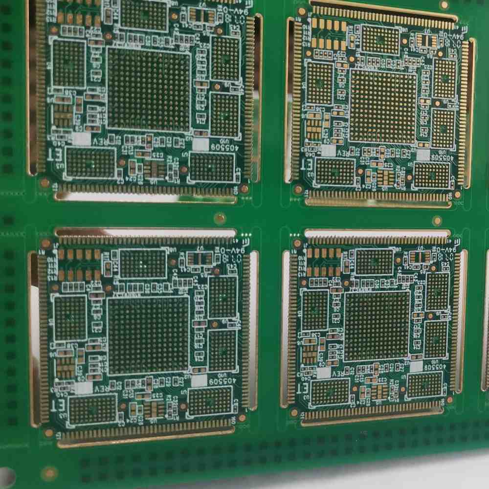
PCB Stackup
The PCB stackup refers to the layer structure of the circuit board. A typical stackup consists of:
- Top and bottom signal layers for component placement and routing
- Power and ground plane layers
- Additional inner signal layers as needed for complex routing
Prepreg or dielectric material separates the conductor layers. Common dielectric materials include FR-4, Rogers, Taconic etc. The stackup is designed based on parameters like layer count, dielectric material, copper thickness and trace/space rules.
| Layer | Function |
|---|---|
| Top | Top Signal Layer |
| GND | Ground Plane |
| PWR | Power Plane |
| L2 | Signal Layer 2 |
| L3 | Signal Layer 3 |
| Bottom | Bottom Signal Layer |
<br>
The number of layers, copper thickness, trace width/spacing depend on PCB complexity, component density and fabrication capability. The designer chooses the optimal stackup based on electrical, thermal, mechanical and cost requirements.
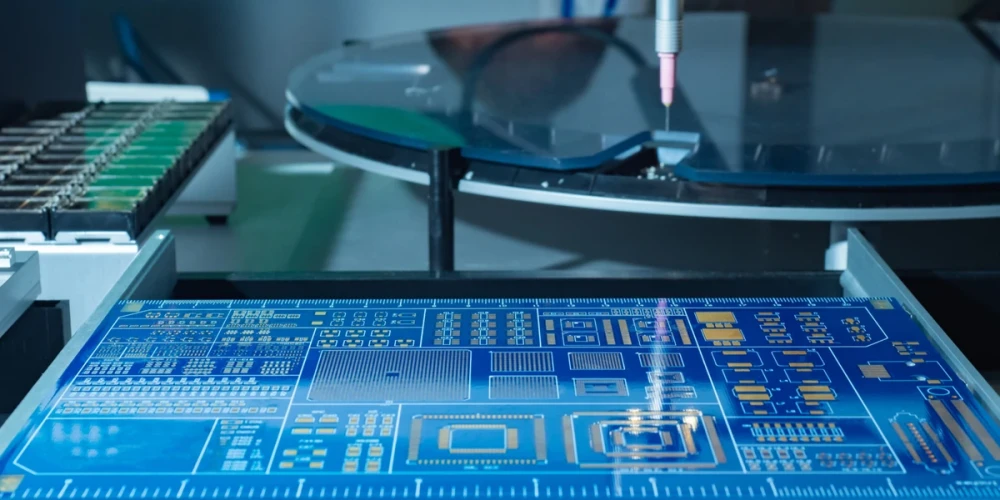
PCB Fabrication Process
Printed circuit boards are fabricated using the following steps:
Solder Mask Application
The solder mask is a coat of polymer material applied on the PCB surface, leaving the solder pads exposed. It acts as insulation between traces and prevents solder bridging.
Surface Finish Plating
The exposed copper is plated with solder or metals like gold, nickel, silver etc. This protects the copper from oxidation and allows soldering.
Silkscreen Printing
Silkscreen layer prints text like component designators, logos, board outline etc as per layout file.
Hole Drilling
Holes are drilled for through-hole component leads and vias for layer interconnections using small drill bits.
Hole Plating
The drilled holes are plated with copper to facilitate through-hole soldering and electrical continuity between layers.
Solder Paste Stencil
A stencil is created with cutouts matching the solder pads. This is used to apply solder paste on pads for SMD soldering.
The fabricated blank PCBs are then tested before being shipped and assembled.
Factors Affecting PCB Fabrication Cost
The fabrication cost depends on the following primary factors:
- Board size – bigger boards cost more
- Layer count – additional layers increase cost
- Tighter tolerances – increase cost
- Advanced materials – high frequency boards cost more
- Special processes – like IMPCB, HDI, burial vias
- Lead time – rush orders can cost substantially higher
- Quantity – bulk orders get discounted rates
- Testing requirements – full testing versus random sampling
- Certifications – UL, CE, RoHS
Common PCB Design Software
Some commonly used PCB design software tools are:
- Altium Designer
- Cadence Allegro
- Mentor Graphics Xpedition
- Autodesk Eagle
- CadSoft Eagle
- KiCad
- OrCAD
- Pads PCB
- Altium CircuitMaker
- DipTrace
- EasyEDA
Altium Designer, Cadence Allegro and Mentor Graphics Xpedition are advanced tools used for complex PCBs. Autodesk Eagle, KiCad are popular for hobbyist and simple boards. Web-based tools like EasyEDA, DipTrace allow online PCB design.
FQA
What is the difference between a PCB layout and schematic?
The schematic is the logical diagram showing the component connectivity. The PCB layout translates the schematic into the physical board with components placed and tracks routed.
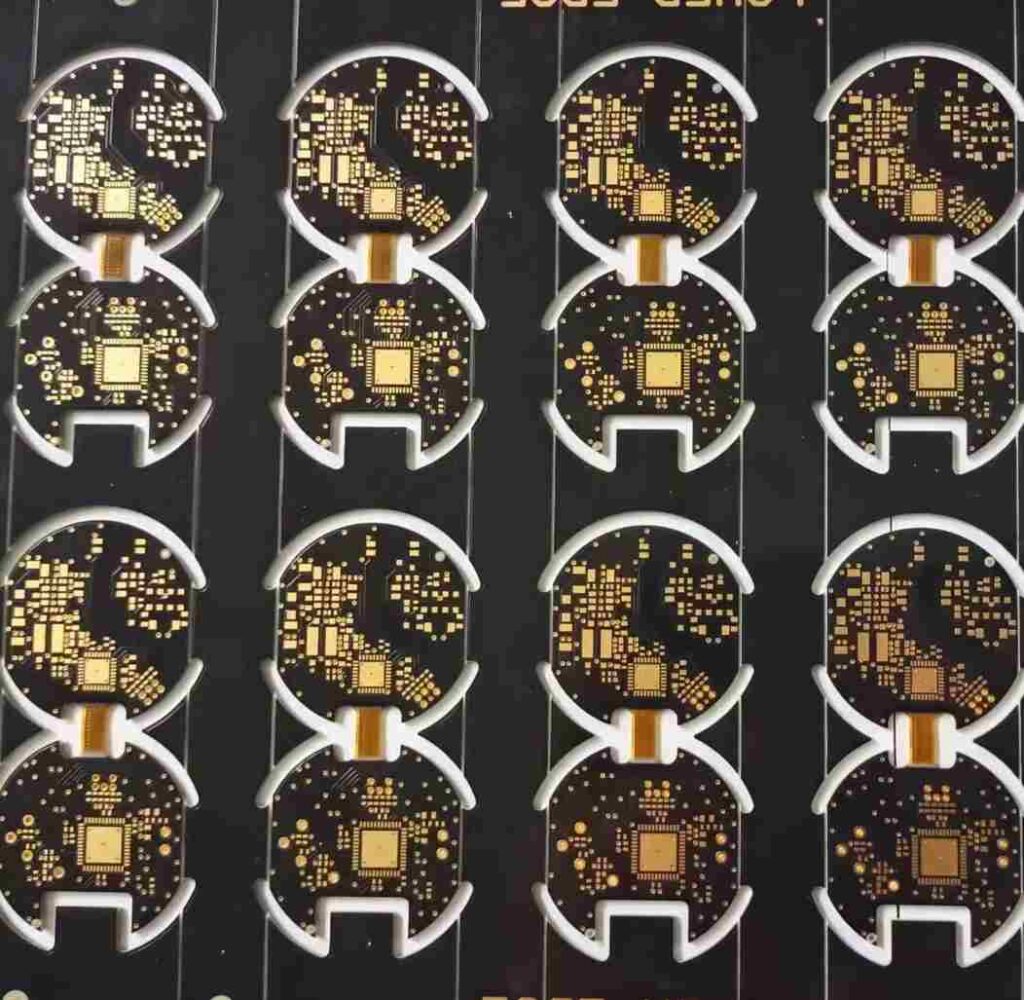
What are the different types of PCBs based on materials?
The common types are:
- FR-4 – Most widely used. Made of woven fiberglass and flame resistant epoxy resin.
- High frequency – Uses PTFE, ceramic, polyimide for high speed signals. E.g: Rogers, Taconic.
- Flexible – Uses polyimide materials. Can flex and bend.
- Aluminum – Suitable for high thermal dissipation.
- Rigid-Flex – Combination of rigid and flexible PCBs.
What is the minimum trace width and spacing that can be acheived?
For standard PCB fabrication processes, the typical minimum trace/space is:
- 8 mil (0.2mm) for 1 oz copper
- 6 mil (0.15mm) for 2 oz copper
For advanced PCBs, widths down to 3-4 mil are possible.
How can EMI emissions be reduced in a PCB design?
EMI can be minimized by:
- Having a continuous ground plane.
- Adding bypass/decoupling capacitors near ICs.
- Keeping analog and digital circuits separated.
- Using shielded cables or ground planes between layers.
- Adding EMI filters on traces.
- Enclosing boards in metal enclosures.
What are some PCB design guidelines for high speed signals?
Guidelines for routing high speed signals:
- Keep traces as short as possible.
- Avoid 90 degree bends. Use 45 degree mitred bends.
- Match trace impedance to source and load impedance.
- Use ground guard traces between signals.
- Use differential pair routing with tight coupling.
- Add termination resistors at trace ends.
What are the different copper finishes used on PCBs?
Common finishes include:
- HASL (Hot air solder leveling) – Applies a solder coating. Most common and cost effective.
- Immersion Silver – Coats traces with silver. Better conductivity than HASL.
- Immersion Tin – Applies a matte tin finish. More solderable than HASL.
- ENIG (Electroless Nickel Immersion Gold) – Applies gold over nickel for corrosion resistance.
- OSP (Organic Solderability Preservative) – An organic coating to protect copper from oxidation.
What are burried vias in PCBs?
Buried vias are holes that connect inner layers without extending to the outer surfaces. This helps reduce layer usage by avoiding stub traces. It also minimizes drilling. But they add cost and require advanced processes.
How can heat dissipation be improved in a PCB design?
Methods to improve thermal performance:
- Use thermal pads or vias to connect components to ground/power planes to spread heat.
- Add thermal reliefs under pads to reduce heat transfer to traces.
- Use wider copper fills around hot components.
- Add extra copper planes if needed solely for heat spreading.
- Use thicker copper layers and multiple plane layers to spread heat.
What are the inspection/testing methods used to verify PCB fabrication quality?
Testing methods include:
- Visual inspection – Checks for visible defects under microscope.
- Net connectivity test – Checks electrical connectivity of all nets on board.
- ICT (In-circuit test) – Tests board functionality by applying vectors and checking outputs.
- Flying probe – Tests connectivity between nodes with flying probes.
- X-Ray imaging – Looks for flaws in internal layers and vias.
- AOI (Automated Optical Inspection) – Imaging based automated inspection.
- Functional testing – Validating complete board functionality.


Leave a Reply