What is a PCB?
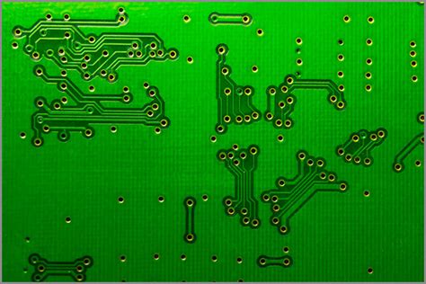
A PCB, or Printed Circuit Board, is a fundamental component in modern electronics. It is a flat board made of insulating materials, such as fiberglass or plastic, with conductive pathways etched or printed onto its surface. These pathways, known as traces, connect various electronic components, such as resistors, capacitors, and integrated circuits (ICs), to create a functional electronic circuit.
PCBs come in various sizes, shapes, and complexities, ranging from simple single-layer boards to complex multi-layer boards with intricate designs. They are used in virtually every electronic device, from smartphones and computers to televisions and industrial equipment.
Types of PCBs
There are several types of PCBs, each with its own unique characteristics and applications:
-
Single-layer PCB: A single-layer PCB has conductive traces on only one side of the board. These boards are the simplest and most cost-effective to manufacture, making them ideal for low-complexity circuits and prototypes.
-
Double-layer PCB: A double-layer PCB has conductive traces on both sides of the board, allowing for more complex circuits and higher component density. These boards are commonly used in consumer electronics, such as smartphones and laptops.
-
Multi-layer PCB: A multi-layer PCB consists of three or more layers of conductive traces, separated by insulating layers. These boards offer the highest level of complexity and component density, making them suitable for advanced applications, such as aerospace and military electronics.
-
Flexible PCB: A flexible PCB is made of a thin, flexible insulating material, such as polyimide, with conductive traces printed onto its surface. These boards can be bent and folded to fit into tight spaces or conform to unique shapes, making them ideal for wearable devices and other applications where flexibility is required.
-
Rigid-Flex PCB: A rigid-flex PCB combines the benefits of both rigid and flexible PCBs. It consists of rigid sections connected by flexible sections, allowing for complex three-dimensional designs and improved reliability in applications with varying mechanical stress.
| PCB Type | Layers | Complexity | Cost | Common Applications |
|---|---|---|---|---|
| Single-layer | 1 | Low | Low | Prototypes, low-complexity circuits |
| Double-layer | 2 | Medium | Medium | Consumer electronics, smartphones, laptops |
| Multi-layer | 3+ | High | High | Aerospace, military, advanced applications |
| Flexible | 1-2 | Low-Medium | Medium | Wearable devices, tight spaces |
| Rigid-Flex | 2+ | High | High | Complex 3D designs, high-reliability applications |
PCB Manufacturing Process
The PCB manufacturing process involves several steps, each requiring precision and attention to detail to ensure a high-quality final product.
1. Design and Layout
The first step in PCB manufacturing is designing the circuit and creating a digital layout using specialized software, such as Altium Designer or KiCad. The layout includes the placement of components, traces, and other features, such as vias and mounting holes.
2. Printing the PCB Pattern
Once the design is finalized, the PCB pattern is printed onto a copper-clad laminate using a process called photolithography. This involves applying a light-sensitive resist to the copper surface, exposing it to UV light through a photomask with the PCB pattern, and developing the resist to remove the exposed areas.
3. Etching
After the PCB pattern is printed, the unwanted copper is removed through an etching process. The board is immersed in an etchant solution, typically ferric chloride or ammonium persulfate, which dissolves the exposed copper, leaving only the desired traces and features.
4. Drilling
Holes are drilled into the PCB to accommodate through-hole components and provide electrical connections between layers in multi-layer boards. This is done using specialized drilling machines with high-speed, high-precision drills.
5. Plating and Coating
To improve the PCB’s durability and protect it from environmental factors, the board undergoes plating and coating processes. These may include:
- Electroplating: A thin layer of copper is deposited onto the traces and through-holes to improve conductivity and durability.
- Solder mask application: A protective coating is applied to the PCB surface, leaving only the exposed pads and through-holes for soldering.
- Silkscreen printing: Text, logos, and other markings are printed onto the PCB surface for identification and assembly purposes.
6. Solder Mask and Silkscreen
In this step, a solder mask is applied to the PCB to protect it from oxidation and prevent solder bridges during the assembly process. The solder mask is typically green, but other colors are available. A silkscreen layer is then added to label components, connectors, and other important features on the PCB.
7. Surface Finish
The exposed copper pads and through-holes receive a surface finish to protect them from oxidation and improve solderability. Common surface finishes include:
- HASL (Hot Air Solder Leveling): A thin layer of solder is applied to the pads and through-holes, creating a flat, solderable surface.
- ENIG (Electroless Nickel Immersion Gold): A layer of nickel is deposited onto the copper, followed by a thin layer of gold, providing excellent solderability and durability.
- OSP (Organic Solderability Preservative): A thin, organic coating is applied to the copper to protect it from oxidation and maintain solderability.
8. Electrical Testing
After the PCB is manufactured, it undergoes electrical testing to ensure that all connections are correct and the board functions as intended. This may include:
- Flying probe testing: A set of mobile probes checks the continuity and isolation of each net on the PCB.
- Bed-of-nails testing: The PCB is placed on a fixture with spring-loaded pins (nails) that make contact with the board’s test points, allowing for rapid testing of multiple boards.

PCB Assembly
Once the PCB is manufactured, it is ready for assembly. The assembly process involves placing and soldering components onto the board to create a functional electronic device.
1. Component Placement
Components are placed onto the PCB using automated pick-and-place machines or by hand for smaller batches and prototypes. Surface-mount components are placed directly onto the pads on the PCB surface, while through-hole components are inserted into the drilled holes.
2. Soldering
After the components are placed, the PCB is soldered to create electrical connections between the components and the traces. Soldering methods include:
- Wave soldering: The PCB is passed over a wave of molten solder, which flows onto the pads and through-holes, creating a connection between the components and the traces. This method is primarily used for through-hole components.
- Reflow soldering: Solder paste, a mixture of tiny solder particles and flux, is applied to the pads using a stencil. The components are then placed onto the solder paste, and the entire board is heated in a reflow oven, melting the solder and creating a connection. This method is used for surface-mount components.
3. Inspection and Testing
After soldering, the assembled PCB undergoes visual inspection and electrical testing to ensure that all components are correctly placed and soldered and that the board functions as intended. This may include:
- Automated optical inspection (AOI): A camera-based system checks for missing or misaligned components, solder bridges, and other defects.
- X-ray inspection: X-ray imaging is used to inspect solder joints and other internal features that are not visible from the surface.
- Functional testing: The assembled PCB is powered on and tested to ensure that it performs according to its specifications.

PCB Design Considerations
When designing a PCB, several factors must be considered to ensure optimal performance, reliability, and manufacturability.
1. Circuit Schematic
The first step in PCB design is creating a circuit schematic, which is a graphical representation of the electronic components and their connections. The schematic should be clear, well-organized, and follow standard conventions for symbols and labeling.
2. Component Selection
Choosing the right components is crucial for the performance and reliability of the PCB. Factors to consider when selecting components include:
- Electrical specifications: Ensure that the components meet the required voltage, current, and power ratings for the circuit.
- Package type: Choose components with package types that are compatible with the PCB manufacturing and assembly processes, such as surface-mount or through-hole.
- Availability: Consider the availability and lead time of components to avoid delays in production.
3. PCB Layout
The PCB layout is the physical arrangement of components and traces on the board. A well-designed layout is essential for optimal signal integrity, power distribution, and thermal management. Key considerations include:
- Component placement: Place components in a logical and organized manner, minimizing the distance between related components and avoiding physical interference.
- Trace routing: Route traces efficiently to minimize signal reflections, crosstalk, and electromagnetic interference (EMI). Use appropriate trace widths and spacing based on the signal requirements and PCB manufacturing capabilities.
- Power and ground planes: Use dedicated power and ground planes to provide low-impedance paths for power distribution and reduce noise.
- Thermal management: Consider the heat generated by components and design the PCB layout to facilitate heat dissipation, such as by using thermal vias or adding heatsinks.
4. Design for Manufacturing (DFM)
Design for Manufacturing (DFM) is the practice of designing PCBs with the manufacturing process in mind, aiming to reduce costs, improve yields, and ensure reliability. Key DFM considerations include:
- Minimum feature sizes: Adhere to the minimum trace widths, spacing, and drill sizes specified by the PCB manufacturer to ensure manufacturability.
- Panelization: Design the PCB to be efficiently panelized, allowing for multiple boards to be manufactured on a single panel to reduce costs.
- Testability: Include test points and other features that facilitate automated testing and inspection during manufacturing.

PCB Testing and Inspection
Thorough testing and inspection are essential to ensure the quality and reliability of PCBs throughout the manufacturing and assembly processes.
1. In-Circuit Testing (ICT)
In-Circuit Testing (ICT) is a method of testing individual components and their connections on an assembled PCB. It involves using a bed-of-nails fixture to make contact with the board’s test points and applying electrical signals to verify the presence, orientation, and functionality of each component.
2. Flying Probe Testing
Flying probe testing is an alternative to ICT that uses mobile probes to check the continuity and isolation of each net on the PCB. This method is more flexible than ICT, as it does not require a dedicated test fixture, but it is generally slower and more expensive.
3. Boundary Scan Testing
Boundary scan testing, also known as JTAG (Joint Test Action Group) testing, is a method of testing the interconnections between digital components on a PCB. It involves using a special test access port (TAP) on each component to control and observe the state of its input and output pins, allowing for the detection of shorts, opens, and other faults.
4. Functional Testing
Functional testing involves powering on the assembled PCB and verifying that it performs according to its specifications. This may include testing the board’s response to various input signals, measuring its output signals, and checking for any abnormal behavior or performance issues.
5. Environmental Testing
Environmental testing is used to evaluate the PCB’s ability to withstand various environmental conditions, such as temperature, humidity, vibration, and shock. This is particularly important for PCBs used in harsh environments, such as industrial or automotive applications.
PCB Troubleshooting and Repair
Despite thorough testing and inspection, PCBs may still experience failures or malfunctions during operation. Troubleshooting and repairing PCBs requires a systematic approach and specialized tools and techniques.
1. Visual Inspection
The first step in troubleshooting a faulty PCB is to perform a visual inspection, looking for any obvious signs of damage, such as:
- Burnt or discolored components
- Cracked or broken PCB substrate
- Lifted or missing traces
- Cold or fractured solder joints
2. Continuity and Isolation Testing
Continuity and isolation testing involve using a multimeter or other test equipment to check for shorts, opens, and other faults in the PCB’s traces and connections. This can help identify the location and nature of the fault, guiding the repair process.
3. Component Testing
Individual components on the PCB can be tested using various methods, such as:
- In-circuit component testing: Using a multimeter or oscilloscope to measure the component’s electrical characteristics while it is still soldered to the PCB.
- Out-of-circuit component testing: Removing the component from the PCB and testing it using dedicated component testers or bench-top equipment.
4. Rework and Repair
Once the fault has been identified, the PCB can be repaired using various rework and repair techniques, such as:
- Soldering: Removing and replacing faulty components, repairing damaged solder joints, or adding jumper wires to bypass damaged traces.
- Trace repair: Using conductive epoxy, copper tape, or wire to repair damaged or lifted traces.
- Conformal coating: Applying a protective coating to the repaired area to improve its durability and insulation properties.
FAQ
1. What is the difference between a PCB and a PCBA?
A PCB (Printed Circuit Board) is the bare board with copper traces and pads, while a PCBA (Printed Circuit Board Assembly) is a PCB with components soldered onto it, forming a complete Electronic Assembly.
2. What are the advantages of using a PCB over other wiring methods?
PCBs offer several advantages over other wiring methods, such as point-to-point or wire-wrap:
- Compact and lightweight design
- Improved reliability and consistency
- Reduced electromagnetic interference (EMI)
- Faster and more efficient assembly
- Lower production costs for high volumes
3. What is the purpose of a solder mask on a PCB?
A solder mask is a protective coating applied to the PCB surface, leaving only the exposed pads and through-holes for soldering. Its main purposes are:
- Preventing solder bridges and short circuits during assembly
- Protecting the copper traces from oxidation and environmental damage
- Providing electrical insulation between adjacent traces
- Improving the PCB’s aesthetic appearance
4. What is the difference between surface-mount and through-hole components?
Surface-mount components are designed to be soldered directly onto the pads on the PCB surface, while through-hole components have leads that are inserted into drilled holes and soldered on the opposite side of the board. Surface-mount components are generally smaller and better suited for high-density designs, while through-hole components are more robust and easier to handle for manual assembly.
5. What is the role of a Gerber file in PCB manufacturing?
A Gerber file is a standard format used to represent the PCB design data for manufacturing. It contains information about the copper layers, solder mask, silkscreen, and other features of the PCB. Gerber files are generated from the PCB design software and sent to the PCB manufacturer, who uses them to create the photomasks and guide the manufacturing process.
Conclusion
PCBs are essential components in modern electronics, providing a reliable and efficient means of interconnecting electronic components. Understanding the fundamentals of PCB design, manufacturing, assembly, and testing is crucial for anyone involved in the development or production of electronic devices.
By following best practices in PCB design, such as careful component selection, efficient layout, and adherence to manufacturing guidelines, designers can create high-quality, reliable PCBs that meet the requirements of their intended application. Thorough testing and inspection during manufacturing and assembly help ensure that PCBs are free from defects and perform as expected.
When PCBs do experience failures or malfunctions, a systematic approach to troubleshooting and repair can help identify and resolve issues quickly and effectively. This involves visual inspection, continuity and isolation testing, component testing, and various rework and repair techniques.
As electronics continue to evolve and become more complex, the importance of PCBs in enabling these advancements cannot be overstated. By staying up-to-date with the latest technologies, techniques, and best practices in PCB design and manufacturing, engineers and technicians can continue to push the boundaries of what is possible in the world of electronics.


Leave a Reply