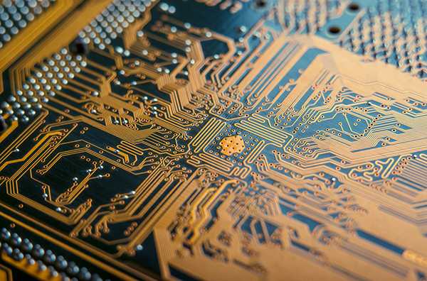
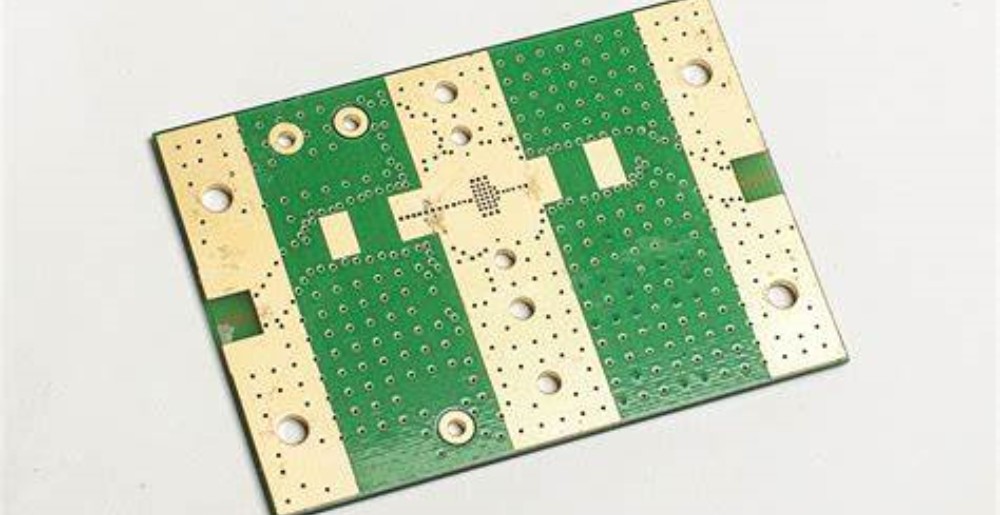
Introduction
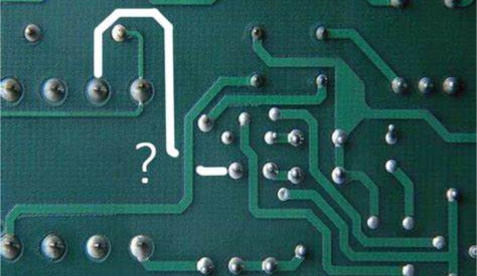
A blind via is a hole that connects different layers of a printed circuit board (PCB) without going all the way through the entire board. Blind vias are used to route connections between layers that are not on the outer surfaces of the PCB. The fabrication process for creating blind vias in PCBs can vary somewhat depending on the manufacturer, but generally involves drilling, metallization, imaging, and other steps to form the interconnects between layers.
Drilling Blind Vias
The first step in creating blind vias is to drill holes in the PCB at the locations where vertical interconnects are needed between layers. This is typically done with a mechanical or laser drilling machine.
Mechanical Drilling
Most blind vias are produced using mechanical drilling with a computer numeric control (CNC) drill. The drill bit progressively removes material to create a hole with the desired diameter and depth to reach the target layer(s). Mechanical drilling can achieve hole diameters down to around 0.15mm (6 mils). The positional accuracy of holes is usually around 0.05mm.
Laser Drilling
For blind vias with very small diameters below 0.15mm, laser drilling is generally used instead of mechanical drilling. A laser beam ablates (vaporizes) the material to form a hole with very high precision. Laser drilling can produce blind vias with diameters down to around 0.025mm (1 mil), with excellent positional accuracy. The depth control of laser drilling also allows creation of vias with different depths or angles if required.
Metallization of Blind Vias
After drilling, the blind via holes must be metallized to create the actual vertical interconnect between layers. There are various metallization processes used:
Electroless Copper Plating
A common method is to use electroless copper plating to deposit a thin layer of copper onto the inner walls of the blind via holes. This provides a conductive surface for further plating.
Copper Electroplating
Once a thin electroless copper layer is deposited, thicker copper is plated onto the hole walls using electroplating. This fully builds up the metal interconnect between layers. Copper electroplating allows a large amount of copper to be deposited rapidly and uniformly within the via.
Conductive Ink Filling
For certain applications like high density interconnects (HDI), the blind vias may be filled with a conductive ink after metallization. This provides better hole wall conductivity and allows smaller via diameters. The conductive ink is screen printed or jetted into the holes to fill them.
Imaging Blind Vias
Imaging is the process of selectively coating areas of the PCB with photoresist, leaving other areas exposed for etching or plating. For blind vias, it may involve:
Photoresist Application
A liquid photoresist (photosensitive polymer) is applied over the entire PCB surface, including within the drilled blind via holes. The photoresist coats all the metallized hole walls.
Selective Exposure
The areas to remain coated are then exposed to light through a mask. The mask blocks light from the areas to be developed away.
Developing
The board is then developed in a chemical solution, which washes away the unexposed photoresist. This leaves behind a patterned layer of photoresist protecting certain areas.
Tenting Vias
For many PCB manufacturing processes, the photoresist must also remain coated over the blind via holes to “tent” them. This tenting photoresist prevents plating or etching within the vias.
Other Fabrication Processes
Additional PCB fabrication steps like copper electroplating and etching are used to form the conductive traces on each layer. The tenting photoresist over blind vias prevents metal deposition within the holes during these processes.
Once all fabrication is complete, the tenting photoresist is chemically stripped away, opening up the blind vias for connectivity between layers. The PCB panel is then ready for electrical testing, quality inspection, and singulation into individual boards.
Sample Blind Via Process Flow:
- Drill blind via holes with mechanical drill or laser
- Electroless plate thin copper onto hole walls
- Electroplate thicker copper onto hole walls
- Apply liquid photoresist onto all surfaces
- Expose and develop photoresist to form pattern
- Tent photoresist over blind via holes
- Electroplate copper traces on layers
- Chemically etch away unwanted copper
- Strip photoresist, re-exposing blind vias
- Test circuits and inspect quality
- Singulate into individual PCBs
Challenges of Blind Vias
While blind vias provide vertical interconnects without using up surface area, there are some challenges involved:
- Limited Aspect Ratio – The ratio of blind via depth to diameter is restricted based on capabilities of processes like drilling and plating. This limits how many layers can be interconnected.
- Reliability – It can be difficult to get uniform plating thickness along the full depth of deep blind vias, affecting long-term reliability.
- Stack-up – Extensive use of blind vias can make board and layer stack-up more complex during layout.
- Cost – Drilling and metallizing blind vias requires specialized equipment and processes, increasing fabrication costs.
When to Use Blind Vias
Here are some situations where using blind vias would be beneficial:
- Interconnections between internal layers needed, but no components on bottom side of board
- High-density PCB with intense component placement, so minimal surface area for through-hole vias
- Multi-layer board where some layer-to-layer connections don’t require full through-hole vias
- Board with tight impedance control constraints, where back-drilling through-hole vias may be prohibitive
- Only lower-precision drilling alignment is needed for the interconnections
Blind vias are suitable when vertical connections are needed for some internal layers, while maximizing use of surface area and minimizing fabrication costs. The tradeoffs must be weighed against alternatives like back-drilled or filled through-hole vias.
Summary
- Blind vias provide selective vertical interconnections between internal PCB layers without occupying surface space.
- Fabrication involves drilling, metallization, imaging, and other steps to form the buried interconnects.
- Challenges include aspect ratio limitations, reliability concerns, layout complexity, and higher costs than standard through-hole vias.
- Best suited for high-density, multilayer boards where only some internal vertical connections are needed.
Careful design and fabrication is required to leverage the advantages of blind vias while mitigating the potential drawbacks. As PCB technology advances, blind and other microvia solutions will continue improving in capabilities and applications.
Frequently Asked Questions
What are the key advantages of using blind vias?
Some key advantages of using blind vias include:
- They don’t take up space on the outer surfaces of the PCB. This leaves more area for component placement and routing.
- They allow more flexible routing between internal layers without using up surface real estate.
- They help minimize the number of through-holes required on dense, multilayer boards.
- They support greater board miniaturization and integration capabilities.
What are the limitations of laser drilling for blind vias?
Some limitations of laser drilling include:
- Thermal damage – excessive heat can damage dielectric around vias.
- Limited depth capability – lasers may not drill deep enough for high layer count boards.
- Slower process – laser drilling is much slower than mechanical drilling.
- Higher cost – laser systems are more expensive to purchase and operate.
- Limited capacities – laser tools have lower throughput than mass mechanical drilling.
Is filling blind vias necessary? What are the benefits?
Filling blind vias is not always necessary, but offers some benefits such as:
- Improved hole wall conductivity for smaller via diameters.
- Increased surface area for heat dissipation through vias.
- Ability to plate over the vias without voids for higher density patterning.
- Reduced risk of pad lifting stresses due to plating within unfilled holes.
- Avoiding entrapment of processing chemistry inside the holes.
So via filling helps enable higher interconnection density designs.
How are blind vias tested for manufacturing defects?
Some ways blind vias can be tested are:
- Automated optical inspection of via holes for issues like opens or lining defects.
- Cross-sectioning sample vias and examining plating quality under a microscope.
- Using x-ray imaging to check for proper plating through the entire depth.
- Testing via chain resistance using probing or an ohmmeter.
- Performing continuity tests between layers using a multimeter.
- Functional electrical testing of boards to check for electrical connectivity issues.
What design rules should be followed for blind vias?
Some key design rules for blind vias include:
- Controlling minimum annular ring width around vias.
- Limiting the ratio of via depth to diameter.
- Meeting minimum hole size and spacing requirements.
- Avoiding placing vias under critical components liable to be affected by drilling debris.
- Allowing slightly larger capture pads for deeper blind vias to account for positional tolerances.
- Providing sufficient anti-pad clearance around plated through holes.
- Setting restrictions on the number of consecutive layers that can be interconnected.
- Defining acceptable layer transitions to avoid complex stack-ups.
Following manufacturability guidelines provided by your PCB vendor is highly recommended.


Leave a Reply