Overview of PCB Assembly
Printed circuit board (PCB) assembly is the process of soldering electronic components to a PCB to create a functional printed circuit assembly (PCA). It is an essential step in the production of most electronic devices. This guide will walk through the key steps involved in PCB assembly and factors to consider when having your boards assembled.
The PCB Assembly Process
The main steps in PCB assembly include:
- Solder Paste Preparation
- Component Placement
- Solder Reflow
- Cleaning
- Automated Optical Inspection
- Remediation
Additional steps like testing, inspection, and protective coatings may also be required depending on the application.
Key Factors in PCB Assembly
Some of the key factors to consider for your PCB assembly include:
- Board complexity – Number of layers, component density, smallest component size, etc.
- Component types – SMD, through-hole, BGAs, connectors, etc.
- Selecting an assembly partner – Experience, capabilities, quality, costs
- Testing requirements – ICT, flying probe, boundary scan, etc.
- Protection – Conformal coating, potting, enclosures etc.
- Certifications – ISO, IATF 16949, ITAR, etc.
Solder Paste Preparation
Solder paste is a material that allows components to be temporarily adhered to a PCB before permanent soldering. It consists of tiny solder balls suspended in flux. Proper solder paste application is crucial for achieving reliable solder joints.
Solder Paste Printing
Solder paste is applied to a PCB using a stencil and squeegee. The stencil is a thin metal sheet laser cut with apertures mirroring the PCB pad design. Here are some guidelines for paste printing:
- Use a stainless steel stencil with electroformed nickel coating
- Match stencil and pad designs
- Apply even pressure when wiping the squeegee across the stencil
- Use miniature snap-off blades for the squeegee
- Print pastes designed for your process (alloy type, particle size)
Solder Paste Inspection
After print, the solder paste deposits should be inspected:
- Use automated optical inspection (AOI) or microscopic inspection
- Check for proper alignment, offset, bridging, insufficient paste, etc.
- Take corrective actions like reprinting if necessary
Solder Paste Storage
To prevent drying and oxidation, solder paste must be properly stored:
- Store at 0°C to 10°C in tightly sealed jars/cartridges
- Return to storage quickly after printing
- Monitor paste quality and discard if exceeded shelf life
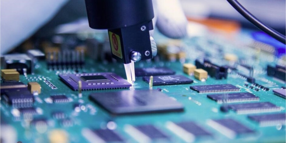
Component Placement
Electronic components must be accurately positioned on the PCB before soldering. Both manual placement and automated pick-and-place machines are used.
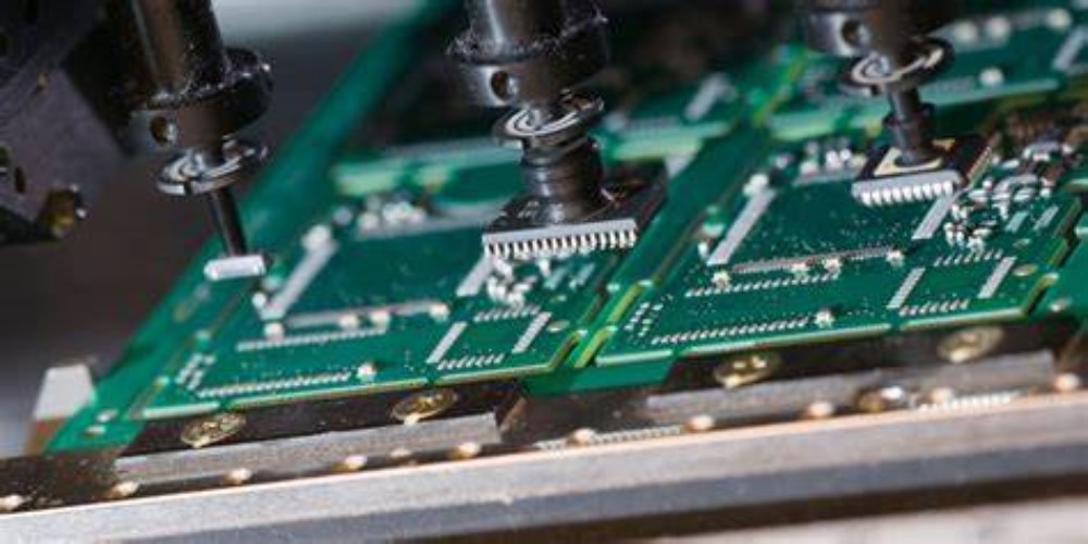
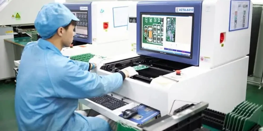
Pick-and-Place Machines
Pick-and-place machines automate the component placement process for high volume production. They use vacuum nozzles to pick components from reels or sticks and place them on PCBs with precision.
Advantages of using pick-and-place machines:
- High speed and throughput
- Consistent, repeatable, and accurate placements
- Support for broad range of component types and sizes
- Automated optical inspection after placement
- Software optimization of placements
Disadvantages:
- High capital investment cost
- Changeover time between PCB designs
- Potential for damaged components or boards
Manual Placement
For low/medium volume or highly specialized boards, manual component placement may be used. Some tips for manual placement:
- Use tweezers and magnifying lens for small components
- Place adhesive components precisely
- Load boards methodically to avoid mistakes
- Visually inspect all component positions
While slower than automated placement, manual placement allows flexibility and control for complex board assembly.
Solder Reflow
Solder reflow is the process of permanently soldering components to circuit board pads by heating the assembly above liquidus temperature. There are two primary methods of reflow:
Soldering Oven
A convection oven uses heated forced air to uniformly heat the assembly. Advantages include:
- Even heating for consistent solder joint quality
- Flexible batch sizes
- Lower equipment cost
The oven temperature is gradually ramped up following a reflow profile specific to the solder alloy used. Common profiles take 5-8 minutes to fully reflow a board.
Infrared/Vapor Phase Reflow
These systems use IR lamps or condensing vapor to quickly transfer heat energy to the assembly. Benefits include:
- Very rapid reflow cycles (~2 min)
- Excellent thermal control for small components
- Minimal oxidation compared to convection
The boards move on a conveyor under the IR lamps or through the vapor phase chamber. Precise profiling is programmed based on board design.
Cleaning
All flux residues must be removed after soldering to prevent corrosion or electrical shorts. Common cleaning methods:
Aqueous Washing
PCBs are sprayed with water or a mild solvent to remove ionic contaminants. Benefits:
- Environmentally friendly
- Efficient removal of flux and paste residues
- Widely available cleaning equipment
Key is using high purity water and properly drying boards after washing.
Semi-Aqueous Washing
A mix of solvent and water is sprayed at high pressure. Used for boards contaminated with conformal coatings or challenging glob top encapsulants.
Solvent Cleaning
Special solvents rapidly dissolve flux residues. Widely used for advanced PCBs, but restricted by environmental regulations in some regions.
Plasma/Ionized Gas Cleaning
Energized gases break down and displace surface contaminants. Non-contact process avoids component damage.
Automated Optical Inspection
AOI machines capture high resolution images of assembled boards and use sophisticated algorithms to analyze solder joints, component placement, markings, and more. AOI identifies defects early and prevents further processing of bad boards.
Typical AOI checks:
- Missing or misaligned components
- Insufficient or excessive solder
- PCB damage, nicks, or scratches
- Violations of minimum clearance
- Correct polarity of polarized components
- Presence of foreign objects
- Marking legibility
By automating inspection, AOI improves quality, reduces escaped defects, and decreases human inspection time.
Remediation
Defects found during AOI or other testing must be reworked or replaced. Common repair methods:
Manual Rework
Using soldering irons, hot air tools, and microscopes, technicians can safely remove, replace, and resolder defective components. Appropriate for small volumes or large components unsuitable for auto-replacement.
Automated Component Placing
Special machines remove defective parts and precisely place new components onto boards without damage. Efficient for mid to high volume repairs.
Depanelization and Component Replacements
On panels with duplicated circuitry, bad components can simply be cut off the panel and replaced with a new replicated board section using soldering or connectors.
Board Repair and Redistribution Services
For systemic design or production issues causing widespread defects, it can be most cost effective to ship boards to specialized repair depots for reworking and salvaging.
Protective Coatings and Encapsulants
For boards exposed to demanding mechanical or environmental conditions, protective materials are applied after assembly:
Conformal Coatings
Thin polymeric films (1-75 um) conformally coat the assembled PCB to prevent corrosion and leakage currents. Variants include acrylic, silicone, urethane, and parylene. Applied via spraying, dipping or automated selective coating.
Potting Compounds
Thick liquid resins (2-5mm) are dispensed to totally encapsulate components. Provide excellent vibration, impact, and splash resistance. Two-part heat cure silicones and epoxies are commonly used.
Ruggedizing Enclosure
Aluminum, steel, or plastic cases shield the PCB from dust, water, and physical damage. Components are mounted to the enclosure using adhesives, standoffs, or fasteners. Provides complete environmental sealing.
Testing and Certification
Multiple testing stages validate PCB assembly quality:
In-Circuit Testing
ICT fixtures contact test points to check component logic, continuity, and analog performance at speed. Catches bad solder joints, wrong components, misloads, etc.
Flying Probe Testing
Lower cost alternative to ICT using “bed of nails” spring-loaded probes to access both sides of the PCB. Limited to boards with sufficient exposed test pads.
Functional Testing
Validates complete board operation by powering on and stimulating inputs while monitoring outputs and performance to datasheet specifications.
Environmental Stress Screening
Accelerated testing for combined temperature, vibration, voltage, etc. to uncover latent defects and validate robustness.
Regulatory Compliance
Third-party agencies certify assembled boards meet safety and emissions standards like CE, FCC, UL, IECEE, RCM.
Choosing a PCB Assembly Partner
Key factors when selecting an electronics manufacturing services (EMS) partner for PCB assembly:
- Technical capabilities – Evaluate assembly technologies, component range, testing/inspection equipment, repair capabilities, certifications, etc.
- Quality – Review process controls, quality management system, continuous improvement practices, defect rates, etc.
- Volume scalability – Assess ability to scale from prototypes to high volume production.
- Cost – Get comprehensive quotes accounting for materials, testing, overhead, etc.
- Lead times – Verify ability to meet delivery targets and adjust capacity.
- Global footprint – For international production, assess locations and compliance.
- Robust supply chain – Vet suppliers, inventory, and procurement practices.
- Design support – Collaboration on DFM, test development, troubleshooting etc.
Taking the time to thoroughly assess potential EMS partners helps ensure you select one with the end-to-end capabilities to meet your specific PCB assembly needs.
Conclusion
PCB assembly transforms bare printed circuit boards into fully functional electronic assemblies. While the soldering process may seem straightforward, each step from paste printing to final protective coatings requires careful process controls to produce a reliable, high-quality board assembly. Working with an experienced EMS provider equipped with the latest assembly technologies and quality systems is key to achieving optimized, defect-free results. This guide covers the essential PCB assembly process steps and considerations to help you successfully carry a design from prototype through volume production.
Frequently Asked Questions
What are the main differences between through-hole and surface mount PCB assembly?
The main differences are:
- Component types – Through-hole uses axial and radial leaded components, SMT uses smaller chip components.
- Board density – SMT allows much higher component density and miniaturization.
- Soldering methods – Through-hole requires point-to-point soldering, SMT uses reflow ovens.
- Automation – SMT is better suited for automated pick-and-place assembly.
- Rework – Replacing defective through-hole components is mechanically easier.
- Cost – Higher capital investment for SMT, lower component cost.
How are very small 0201 and 01005 components handled in SMT assembly?
Miniature 0201 (0.6mm x 0.3mm) and 01005 (0.4mm x 0.2mm) components require specialized handling:
- High precision pick-and-place machines with cameras and tweezers.
- Microscopic visual inspection.
- Solder paste printing process optimized for ultra-fine pitch.
- Package-on-package stacking configurations.
- Reflow profiles optimized for small thermal mass.
- Automated optical inspection with high magnification.
The assembly process must be finely tuned to accommodate smaller geometries.
What are some methods for protecting PCB components from harsh environments?
Common PCB protection methods include:
- Conformal coatings – Thin polymer layers prevent corrosion and leakage.
- Potting compounds – Thick resins encapsulate against vibration and moisture.
- Rugged enclosures – Metal or plastic cases shield against dust and impact.
- Hermetic sealing – Air-tight ceramic or metal enclosures prevent gas exchange.
- Underfill and encapsulants – Protect chip-scale components.
The method used depends on the specific environmental conditions the PCB must withstand.
How are PCB assembly defects remediated?
Common remediation methods for PCB assembly defects include:
- Manual rework – Use of soldering irons and microscopes to remove and replace components.
- Automated replacing – Machines remove defective parts and place replacements.
- Depaneling – Remove defective sections of arrays and replace.
- Board repair services – Companies specialize in reworking defects.
- Scraping – Severely defective boards must be discarded and recycled.
The approach depends on defect type, location, and volume considerations.
What design considerations help optimize manufacturability during PCB assembly?
Some PCB design tips to facilitate assembly include:
- Allow sufficient clearance around components.
- Use standard component packages and sizes.
- Include fiducials for accurate component placement.
- Allow access to both sides of the board.
- Incorporate testpoints for validation.
- Follow manufacturer design rules and guidelines.
Taking assembly requirements into account during design improves manufacturing yield.


Leave a Reply