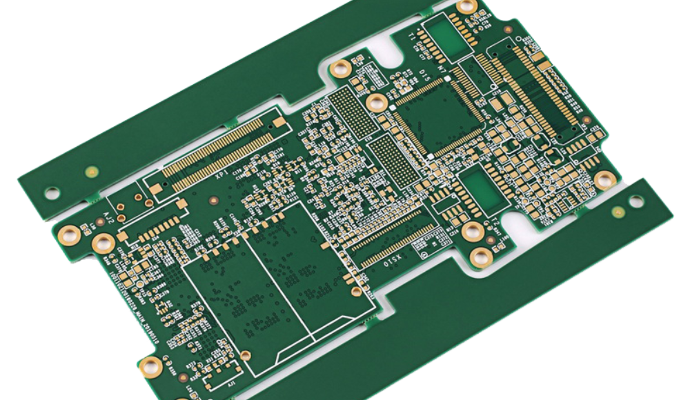
Introduction to High Density Interconnect (HDI) PCBs
High density interconnect (HDI) PCBs are printed circuit boards with a higher wiring density than conventional PCBs. They enable the miniaturization of electronic devices by accommodating a high number of interconnects in a small surface area.
Some key characteristics of HDI PCBs are:
- Extremely fine lines and spaces. Track widths and spacings of 4 mils or below.
- Multiple circuit layers. Up to 20 conductive layers.
- Laser drilled microvias. Microvias with diameters less than 6 mils connecting different layers.
- Thin dielectric layers. Layer thickness as low as 3 mils.
- High component density. More SMT components per unit area than conventional PCBs.
The main benefits of HDI PCBs include:
- Miniaturization of products. HDI allows for more functionality in smaller products.
- Increased signal speed. Thinner dielectric layers mean shorter signal transition times.
- Noise reduction. Ground planes between signal layers block cross-talk.
- Reliability. Less chance of via failure due to smaller drill diameters.
- Design flexibility. More routing channels between layers for complex layouts.
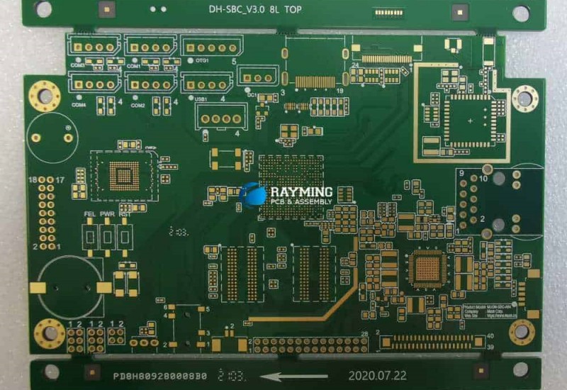
Some common applications of HDI PCBs include smartphones, tablets, wearables, medical devices, aerospace avionics and high-speed communications. The high performance and small size make them suitable for compact, feature-rich consumer electronics as well as advanced industrial and military applications.
HDI PCB Design and Layout Considerations
Designing HDI PCBs requires special considerations compared to conventional PCBs:
Board Stackup
The board stackup refers to the sequence of conductive and dielectric layers in the PCB. For HDI boards, a typical stackup has:
- Several thin dielectric core layers separated by ground planes. This provides multiple routing channels.
- Thin dielectric buildup layers on the outer surfaces for external trace routing.
- Several thick power plane layers to handle high current requirements.
The key is minimizing dielectric thickness between routing layers while maintaining adequate insulation between conductors. Typical core dielectrics are 3-4 mils while buildup dielectrics are 1-2 mils.
Via Structures
HDI PCBs use multiple types of vias for vertical interconnects:
- Microvias: Less than 6 mil diameter, used to connect buildup layers or adjacent core layers. Enable high interconnect density.
- Blind/buried vias: Connect inner layers without spanning full board thickness. Allow for complex routing.
- Through-hole vias: Span entire board thickness and connect components. Have larger diameters than microvias.
The via distribution across layers significantly impacts design complexity, manufacturability and cost.
Routing Channels
With multiple thin cores and buildup layers, HDI boards offer many parallel routing channels or layers for traces. This facilitates routing complex designs while meeting length matching and impedance requirements.
Channel direction alternates with each layer to enable efficient breakout of dense ball grid array packages. Non-functional connections may be required between layers to simplify routing.
Controlled Impedance Lines
Controlled impedance lines with matched lengths are essential for multi-gigabit data signals. Tighter impedance tolerances like +/- 5% are necessary due to thinner dielectrics between reference planes.
Differential pairs must be properly routed with consistent spacing to control crosstalk. Matched line lengths reduce signal skew. Simulations help verify impedance antes the board is manufactured.
Board Outline and Panelization
HDI boards have a high cost per unit area due to the complex layer stackup and laser drilling. To reduce cost, HDI PCBs are fabricated in panel sizes up to 24″ x 24″ or larger.
V-scoring or routing is used to separate individual boards from the panels. Stress relief features may be added along tooling rails and board edges to prevent warping. Panelization considerations impact placement of individual PCBs.
HDI PCB Design and Layout Process
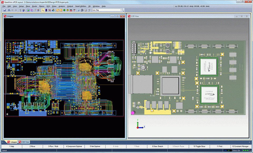
The design process for an HDI PCB involves:
Package Selection
High pin count packages like BGAs with 0.8mm pitch or less are commonly used. The I/O density matches well with HDI capabilities. Package selections should consider HDI design and assembly complexity.
Create Board Stackup
Define dielectric materials, layer count, sequence and thicknesses based on electrical, thermal and mechanical requirements. Dielectric materials include epoxy, polyimide, liquid crystal polymer (LCP), PTFE composites.
Schematic Capture
Create the circuit schematic showing components and connectivity. Schematic driven layout is preferable for HDI designs due to their complexity.
Create Board Outline
Based on selected packages, define a board outline that meets mechanical requirements and panelization goals. Account for any edge connectors or other peripheral features.
Place Major Components
Position major IC components on the board outline. Ensure adequate clearance between heat generating components.
Route Critical Traces
Manually route board traces requiring controlled impedance or length matching. Simulate impedance to match target.
Author Netlist
Generate a netlist defining component pin-to-pin connectivity in the PCB layout tool.
Generate Power Planes
Define power and ground planes according to the stackup. Ensure adequate clearance from plane splits to pads and vias.
Autoroute Remaining Traces
Use autorouter tools to connect all pins and components. Follow good autorouting practices specific to HDI boards.
Add Finishing Touches
Manually fix any remaining design rule violations or unrouted connections. Add text, logos, assembly drawings and fabrication notes as required.
Design Rule Check
Verify the finished layout meets all spacing and clearance requirements for the selected PCB fabricator. Resolve any errors before releasing the design files.
Release Manufacturing Files
After validation, release the completed design data including Gerbers, drill files, netlists, fabrication drawings and assembly instructions.
HDI PCB Fabrication Process
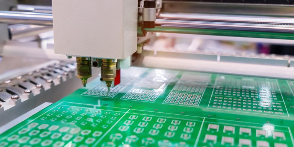
Fabricating HDI PCBs requires advanced manufacturing capabilities and precision processes:
Copper Foil Lamination
Bonds the dielectric core layers and copper foils that will form inner plane layers using high heat and pressure:<table> <tbody> <tr> <td>Dielectric Materials</td> <td>Epoxy, polyimide, PTFE composites, LCP</td> </tr> <tr> <td>Foil Thickness</td> <td>0.5 to 3 oz (18-100 μm) typical</td> </tr> <tr> <td>Bonding Pressure </td> <td>Up to 500 psi at 180-200°C</td> </tr> </tbody> </table>
Photolithography
Patterns the copper layers by selectively removing copper to form interconnects and pads:<table> <tbody> <tr> <td>Lamination</td> <td>Apply photoresist coating</td> </tr> <tr> <td>Exposure</td> <td>Expose photoresist per circuit image</td> </tr> <tr> <td>Developing</td> <td>Remove exposed photoresist</td> </tr> <tr> <td>Etching</td> <td>Chemically etch to remove copper</td> </tr> <tr> <td>Stripping</td> <td>Remove remaining photoresist</td> </tr> </tbody> </table>
Dielectric Buildup
Adds thin dielectric layers on top of the fabricated core to form additional routing layers:
- Uses liquid dielectric materials that are coated, dried and cured.
- Thickness can be precisely controlled to 1-2 mil.
- Enables very dense trace geometries.
Microvia Formation
Creates vertical interconnects between layers with laser drilling:
- Excimer lasers drill small vias typically 25-60 μm in diameter.
- Precise depth control to avoid hitting inner layers.
- Laser systems can drill over 100,000 vias per hour.
Plating and Metallization
Deposits conductive metals to form traces and prepare surfaces:
- Electroless copper followed by electrolytic copper builds up vertical interconnects.
- Electrolytic copper plates outer layers to desired thickness.
- Finishes like ENIG, immersion gold or OSP protect copper traces.
Solder Masking
Applies epoxy-based coatings to avoid solder bridging and protect circuits:
- Liquid photoimageable solder mask (LPSM) is widely used.
- Screen printing, inkjet printing and spray coating are application methods.
- Provides insulation, mechanical protection and marking.
Routing and Scoring
Separates individual PCBs from the fabrication panel:
- Diamond saws mechanically route or score panels.
- Stress relief features prevent warping or cracking.
- Individual PCBs are then broken or routed out.
Testing and Inspection
Verifies quality and reliability before shipping boards:
- Automated optical inspection detects defects and abnormalities.
- Netlist testing checks for opens, shorts and missing connections.
- Microsectioning confirms proper layer alignment and plating quality.
- Electrical testing validates functioning prior to shipment.
Final Finishing
Applies solder paste, legends and protective coatings as needed for assembly. Boards are then packed and shipped.
HDI PCB Assembly Considerations
Assembling boards with HDI technology also requires specialized capabilities:
- Fine pitch components like 0402 discrete passives and 0.4mm pitch QFNs demand accurate pick-and-place machines.
- Smaller paste deposits and thinner stencils are needed for microvias and fine pad geometries.
- X-ray inspection is used to check for defects such as opens or bridges in the as-assembled board.
- Minimized loop heights and sweeping help mitigate tombstoning when soldering bottom terminated components.
- Reworking and replacing microcomponents requires hot air tools with fine nozzle tips.
HDI assembly resembles typical SMT assembly but with tighter tolerances and process controls to match the board geometries involved. Working with an assembly partner experienced in HDI boards is highly recommended.
Trends and Future Outlook for HDI Technology
Continued miniaturization of electronics is driving increased adoption of HDI PCBs:
Increasing HDI Layer Counts
Manufacturing processes continue improving, allowing greater numbers of thinner dielectric and conductive layers. Already 12+ layer designs are common, with ongoing efforts targeting 20+ layer HDI boards.
Shrinking Microvias and Traces
Laser via diameters below 50 μm and line/space below 2/2 mils are becoming feasible as processes mature. This supports further miniaturization of components and pitches.
Embedding Passive Components
To save space, more passives are being embedded into HDI boards rather than soldered. Transmission lines are also being integrated for RF designs.
Adoption in New Applications
HDI technology is expanding beyond high-end consumer devices into specialized medical, automotive, aerospace, 5G infrastructure and IoT products seeking miniaturization.
While costs are still higher than standard PCBs, HDI provides unmatched interconnect density and will become accessible to more applications as technology progresses.
Conclusion
HDI PCB technology enables designing complex, highly compact boards with multiple fine-geometry routing layers interconnected by microvias. Careful design practices including impedance control, layer stackup and component selection are necessary to utilize HDI capabilities fully. Leading edge manufacturing processes allow fabrication of extremely dense interconnects within and between layers. HDI assembly demands advanced practices as well but facilitates integrating complex ICs and passives. With ongoing improvements in processes and cost reduction, HDI PCBs will become essential for product miniaturization across many industries in the future.
Frequently Asked Questions
What are the key advantages of HDI PCB technology?
The main benefits of HDI PCBs are increased circuit density and miniaturization, improved electrical performance through thinner dielectrics, and design flexibility from additional routing layers. HDI enables packing more functionality into a small PCB area.
What are typical design geometries for an HDI board?
Typical HDI capabilities are line widths/spaces of 2 mils or below, microvias with 5-6 mil diameter, and dielectric thicknesses of 2-4 mils. More advanced designs may reach 1 mil lines or 3 mil microvias.
What fabrication processes are unique to HDI PCBs?
Laser drilling of microvias, thin dielectric buildup layers, and very fine pattern etching allow creating the dense stacked layer structure of HDI boards. Tight process controls are needed for thin materials and high precision.
How should I choose dielectrics for an HDI stackup?
Look for materials with stable, low loss electrical properties. Thermal expansion and compliance are also important. Common picks are hydrocarbon epoxies, polyimides, PTFE composites, and LCP which all meet HDI needs.
What design factors help reduce costs for HDI PCBs?
Using fewer layer transitions, minimizing fine line lengths, controlling skew to avoid length matching, and optimizing panel utilization help lower fabrication costs. Upfront design optimization is key for controlling HDI expenses.


Leave a Reply