Overview of Nan Ya PCB
Nan Ya PCB is a leading printed circuit board (PCB) manufacturer based in Taiwan. Founded in 1982, Nan Ya PCB has over 30 years of experience in the PCB industry and has become one of the top PCB suppliers worldwide.
Some key facts about Nan Ya PCB:
- Headquarters located in Taoyuan, Taiwan
- Employs over 5,000 staff
- Operates 6 manufacturing plants in Taiwan
- Additional factories located in China, Vietnam, and Philippines
- Manufacturing capacity of over 500,000 square meters per month
- Serves customers globally in communication, consumer electronics, automotive, industrial, and medical industries
Nan Ya PCB operates at the forefront of PCB technology and offers a comprehensive range of PCB services including:
PCB Capabilities
- Rigid PCBs
- Flexible PCBs
- Rigid-flex PCBs
- High frequency (RF/microwave) PCBs
- High density interconnect (HDI) PCBs
- Metal core PCBs
- IC substrate PCBs
- High thermal conduction boards
PCB Services
- PCB design and layout
- PCB prototyping and small batch production
- Mass production and assembly
- PCB testing and inspection
- Material analysis and failure analysis
Nan Ya PCB Manufacturing Process
Nan Ya PCB utilizes state-of-the-art facilities and stringent quality control to produce high-quality PCBs cost-effectively. Here is an overview of Nan Ya PCB’s manufacturing process:
Step 1: Engineering and Design
The process starts with front-end engineering (FEED) and PCB design and layout services. Nan Ya PCB works closely with customers on design for manufacturing (DFM) to optimize the PCB design.
Step 2: Prototyping
A prototype PCB is first fabricated to verify the design before full production. This validation process helps reduce errors and ensures the design meets specifications.
Step 3: Production Planning
Detailed production planning is conducted including manufacturing engineering, procurement of raw materials, and resource allocation across production lines.
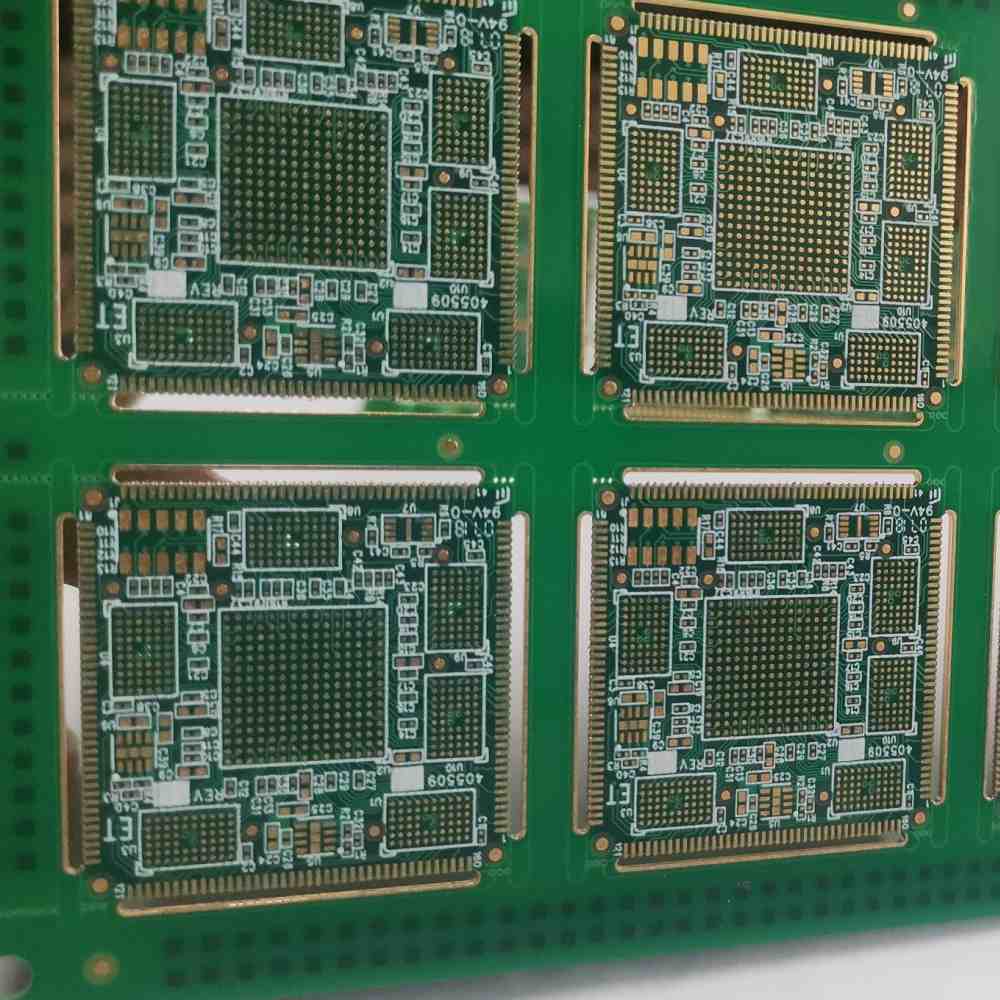
Step 4: Inner Layer Manufacturing
Inner layer circuitry is fabricated first using lithography, etching, and stripping processes. Rigid multilayer boards may have up to 36 layers.
Step 5: Lay Up and Lamination
Inner layers are precisely aligned and laminated together under high temperature and pressure to form a multilayer board.
Step 6: Outer Layer Manufacturing
Outer layers are processed using lithography, etching, stripping, and tin plating. Solder mask and silkscreen are applied.
Step 7: Testing and Inspection
100% testing and inspection is conducted including automated optical inspection (AOI) and electrical testing. X-ray inspection ensures quality.
Step 8: Routing and Scoring
CNC machines rout and score the boards to divide into individual PCBs. Additional finishing steps are completed.
Step 9: Assembly
SMT assembly, cleaning, conformal coating, and other secondary operations are offered.
Step 10: Final Testing
Finished boards undergo a final quality audit and testing before shipment to the customer.
| Manufacturing Process | Details |
|---|---|
| Engineering and Design | Front-end design, layout, DFM |
| Prototyping | Validation of design |
| Production Planning | Manufacturing engineering, procurement, resource allocation |
| Inner Layer Manufacturing | Lithography, etching, stripping |
| Lay Up and Lamination | Layer alignment and lamination |
| Outer Layer Manufacturing | Lithography, etching, plating, solder mask, silkscreen |
| Testing and Inspection | AOI, electrical testing, x-ray |
| Routing and Scoring | CNC routing and scoring |
| Assembly | SMT, conformal coating, other assembly |
| Final Testing | Quality audit and testing |
Nan Ya PCB Quality Control
Nan Ya PCB has industry-leading quality control systems to ensure consistent production of high reliability PCBs:
- ISO 9001 and IATF 16949 certified quality management system
- Comprehensive quality monitoring throughout entire manufacturing process
- Automated optical inspection (AOI) of inner and outer layers
- Rigorous electrical testing and x-ray inspection
- Quality control sampling at multiple process steps
- Reliability testing including thermal stress, vibration, shock, and more
- Strict statistical process control (SPC)
- Continuous improvement through corrective and preventive action
- Customer technical support for quality troubleshooting
By investing heavily in quality control infrastructure and adopting a zero-defect policy, Nan Ya PCB delivers exceptional product quality and reliability.
Nan Ya PCB R&D and Engineering Capabilities
Nan Ya PCB maintains advanced research and development (R&D) and engineering capabilities to support customers with innovative PCB solutions:
- R&D Center: Nan Ya operates a dedicated PCB R&D center focused on developing next-generation PCB technology. Efforts include high frequency, high speed, HDI, and substrate R&D.
- Engineering Support: Nan Ya provides engineering consultation and design support to customers. This includes DFM, DFT, material engineering, stacking analysis, thermal analysis, signal integrity analysis, power integrity analysis, and more.
- Process Development: Nan Ya engages in ongoing process improvement to optimize manufacturing capabilities. Process innovation helps improve product performance, quality, and cost.
- Failure Analysis: Sophisticated failure analysis tools are used to diagnose defects and implement corrective actions. Test capabilities include SEM, FIB, XRF, SAM, and thermal/mechanical/electrical testing.
By combining manufacturing excellence with cutting-edge R&D and engineering, Nan Ya delivers exceptional technical PCB solutions tailored to customer needs.
Nan Ya PCB R&D/Engineering Capabilities
- R&D Center for next-generation PCB technology
- Engineering consultation for design optimization
- Process development and innovation
- Comprehensive PCB failure analysis
- Electrical, mechanical, thermal testing
- SEM, FIB, XRF, SAM analysis tools
Applications of Nan Ya PCBs
Nan Ya PCB supports a highly diverse range of end product applications, including:
Communication
- Networking: Routers, switches, servers
- Wireless: 5G infrastructure, smartphones
- Telecom: Base stations, switches
Consumer Electronics
- Mobile devices
- Laptops, tablets, wearables
- Home appliances
- Gaming devices
Automotive
- Engine control units
- ADAS systems
- Infotainment systems
- Vision systems
Industrial
- Factory automation
- Robotics
- Test and measurement equipment
- IoT devices
Medical
- Patient monitoring systems
- Diagnostic imaging systems
- Therapeutic devices
- Other medical electronics
Nan Ya PCB has unique capabilities to produce advanced PCBs meeting the stringent technical and reliability requirements for cutting-edge electronics across all these markets.
Why Choose Nan Ya PCB?
Here are key reasons to choose Nan Ya PCB as your trusted PCB partner:
- Technology leader – leading edge capabilities in HDI, flexible, substrate, and RF PCBs
- Reliability – flawless quality control and rigorous testing delivers consistent, high reliability PCBs
- Volume production – high-volume manufacturing capacity and capabilities
- Cost competitiveness – excellent value from manufacturing scale and efficiency
- Customer focus – superb technical support and customer service
- Fast turnaround – rapid prototyping through mass production
- Global support – sales and engineering support worldwide
As a tier 1 PCB supplier, Nan Ya PCB offers world-class technology and manufacturing capabilities backed by outstanding customer service and support. Contact Nan Ya PCB today to experience the benefits of partnering with a premier PCB manufacturer.
Frequently Asked Questions
What types of PCBs does Nan Ya manufacturer?
Nan Ya manufactures all major PCB varieties including rigid, flexible, rigid-flex, HDI, high frequency, IC substrates, and more. Complexity ranges from single-sided to 36+ layer boards.
What industries does Nan Ya PCB serve?
Key markets served include communication, consumer electronics, automotive, industrial, medical, aerospace, and military. Nan Ya supports diverse end applications from networking to wearables.
What are Nan Ya PCB’s quality certifications?
Nan Ya PCB is ISO 9001 and IATF 16949 certified. They adopt a zero-defect quality policy through rigorous process controls, inspection, and testing.
Does Nan Ya offer engineering support services?
Yes, Nan Ya provides extensive engineering consultation and analysis including DFM, DFT, signal/power integrity, thermal analysis, and material engineering.
How can I get a quote for Nan Ya PCB manufacturing?
You can obtain a free quote by contacting Nan Ya sales and providing PCB design files or specifications. Nan Ya can also provide design support if needed.


Leave a Reply