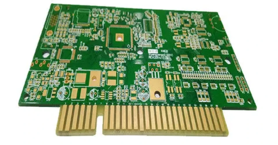
Multilayer metal core printed circuit boards (PCBs) are a specialized type of PCB that have gained popularity in recent years. As the name suggests, these boards contain multiple conductive layers separated by insulating dielectric layers, with a metal substrate at the center acting as a thermal conductor and providing rigidity. Let’s take a deeper look at how multilayer metal core PCBs work and the key considerations when designing and manufacturing them.
What is a Multilayer Metal Core PCB?
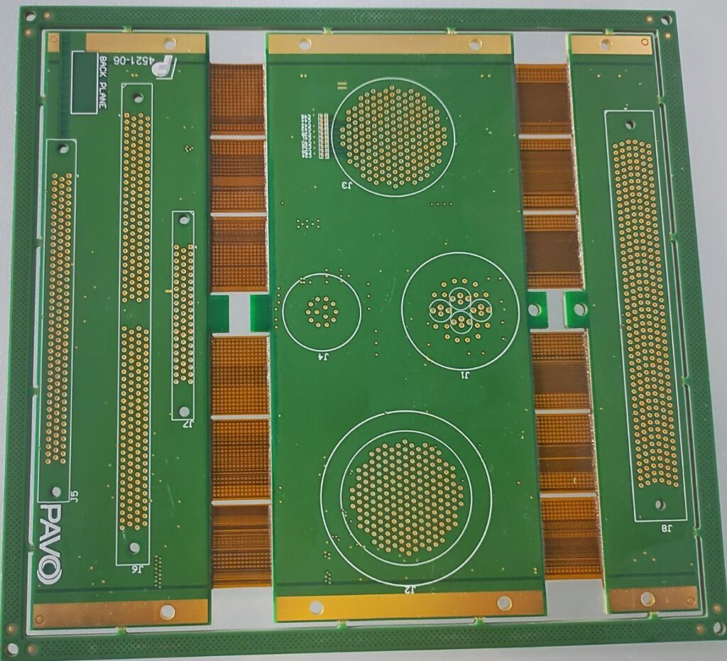
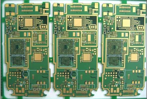
A multilayer metal core PCB consists of the following components:
- Metal core substrate – Typically made of aluminum or copper, this forms the central layer of the PCB. The metal core acts as a heatsink, conducting heat away from the board.
- Dielectric layers – These are insulating polymer layers that separate the conductive layers. Common dielectrics used include polyimide and FR-4.
- Conductive layers – Copper foil layers are laminated onto the dielectric layers to form the conductive portions of the circuitry. There are typically 4-20 conductive layers.
- Solder mask – A coat of epoxy-based paint that protects the copper traces from oxidation and prevents solder bridges from forming.
- Silkscreen – Printed layer for labeling components.
- Plated through holes (PTHs) – Holes drilled through the entire board and plated with copper to allow connections between layers.
- Vias – Plated through holes that connect two or more layers without passing through the entire board.
The combination of multiple conductive layers, dielectric insulation, and a metal core gives multilayer metal PCBs distinct advantages in certain applications which will be explored later. First, let’s look at the manufacturing process.
Manufacturing Process
Multilayer metal core PCBs are fabricated using a complex lamination process. Here are the key steps:
- The metal substrate is pre-treated to activate the surfaces for bonding.
- Layers of dielectric are stacked up. The dielectric layers have cladding of copper foil on one or both sides.
- The stack is aligned and laminated together under heat and pressure.
- Drill holes are made for vias and PTHs. The holes are electroplated to form copper walls.
- Conductive and resistive pastes are screen printed on each layer.
- Various plating and coating processes are used to apply solder mask, silkscreen, and finishes.
- The boards are depanelized by routing/milling.
- Electrical, mechanical, and functional testing is conducted.
- Final boards are shipped to the customer.
The lamination process allows a high degree of precision in constructing boards with multiple layers. Let’s look at some of the design considerations.
Design Considerations
Designing multilayer metal core PCBs requires paying attention to thermal management, signal integrity, and manufacturability. Here are some key considerations:
- Layer stackup – A properly planned layer stackup is critical for routing dense boards. A common approach is to place the power/ground planes close to the metal core for heat spreading, followed by signal layers on the outside. High speed signals are routed on outer layers.
- Trace width and spacing – Narrow traces and spacing are possible, but this increases resistance. Balancing trace width with current levels avoids overheating. A minimum spacing of 4-8 mils between traces is recommended.
- Via design – Vias act as thermal vias conducting heat as well as electrical connections between layers. Using many smaller vias improves heat transfer. Their placement requires attention to avoid interfering with routing.
- Plane gaps – Small gaps may be required in power and ground planes to prevent shorting due to misregistration during lamination. Filling gaps with epoxy avoids issues.
- Component placement – This can significantly impact routing complexity. Critical traces should be as short as possible. Providing access to routing layers for dense areas is key.
- Thermal management – The metal core removes heat, but thermal interfaces, plane design, trace size, and airflow also impact cooling. Thermal modeling early in the design process is recommended.
- EMI/EMC considerations – High speed signals require attention to crosstalk and EMI containment. Noise filters, ground planes, and chassis grounding help meet EMI requirements.
Careful planning following best practices for each aspect is necessary to design multilayer boards successfully.
Applications and Benefits
Some of the key benefits and applications of multilayer metal core PCBs include:
Thermal performance – The metal core provides an excellent heatsink for high power components and circuits. This allows packing dense electronics needing cooling.
Miniaturization – More components and functionality can be fit into a smaller volume vs traditional PCBs.
High frequency performance – Careful layout enables managing high speed signals for RF and microwave circuits.
Power circuits – The board can handle higher current levels safely due to the metal core heatsinking. Multilayer construction provides isolation between circuits.
Noise reduction – Additional shielding against EMI noise is possible through chassis bonding and ground planes.
Mechanical strength – The metal core provides enhanced structural rigidity and resistance to shock/vibration.
These properties make multilayer metal core PCBs ideal for applications like:
- Power electronics – Motor drives, power supplies
- LED lighting
- Automotive electronics
- Industrial controls
- Telecom/RF equipment
- Aerospace/military electronics
In summary, the combination of small size, electrical performance, thermal dissipation, and ruggedness of multilayer metal core PCBs make them an enabling technology across several industries.
Key Manufacturers and Cost Considerations
Some of the leading manufacturers that offer multilayer metal core PCB fabrication include:
- TTM Technologies
- AT&S
- Ibiden
- Tripod Technology
- Unimicron
- Nan Ya PCB
- Cicor
- Sierra Circuits
Cost depends on the complexity and tolerances required. Some guidelines on cost:
- 2-8 layer boards – $2,000 to $15,000 for small batches
- 8 layers – $15,000 to $50,000 for small batches
- Tighter tolerances increase cost
- Advanced materials like ceramic dielectric layers add cost
- High layer counts above 16 layers can range from $50,000 to over $100,000
Discussing requirements in detail with manufacturers is recommended for accurate cost and lead time estimates.
FQA
Here are some frequently asked questions about multilayer metal core PCBs:
What are the typical substrate thicknesses used?
Aluminum core thickness is typically 0.040″, while copper cores range from 0.012″ to 0.024″. Thicker cores improve thermal performance but are heavier.
What dielectrics materials are used?
FR-4 is common for low cost boards. For better thermal transfer, thermally conductive options like polyimide, Isola, and aluminum nitride are used.
What are thermal vias and how do they help?
Thermal vias are holes plated through multiple layers to conduct heat from components to the metal core. Using many smaller vias improves heat spreading.
How many layers can be accommodated?
Up to 20 conductive layers are possible, though 8-12 is more common. More layers allow greater routing density but increase cost.
How are components attached to the board?
SMT components are attached by soldering to pads on the outer layers. Larger components may use thermal adhesives or be soldered to thermal lands connected to the core.
What are the limitations of this technology?
The complexity limits board sizes to around 20″x20″. Warping during lamination can also become a problem with larger boards or tighter tolerances.
Conclusion
Multilayer metal core PCBs enable packing dense electronics into compact, thermally efficient assemblies. The combination of a metal core for heat spreading and multiple layers for circuit routing provide performance not achievable with conventional PCBs. With careful attention to the layout and sound design practices, multilayer metal core boards can be successfully designed and fabricated. As electronics applications demand ever greater power densities, these boards will continue seeing increased adoption across industrial and consumer devices.


Leave a Reply