As electronics become more complex, multi layer printed circuit boards (PCBs) have become increasingly common. Choosing the right multi layer PCB manufacturer is crucial to ensuring your project’s success. This article will guide you through the key factors in selecting a manufacturer and provide recommendations for top multi layer PCB fabricators.
What is a Multi Layer PCB?
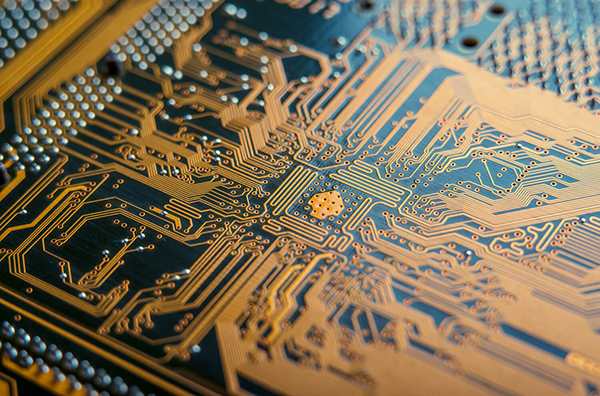
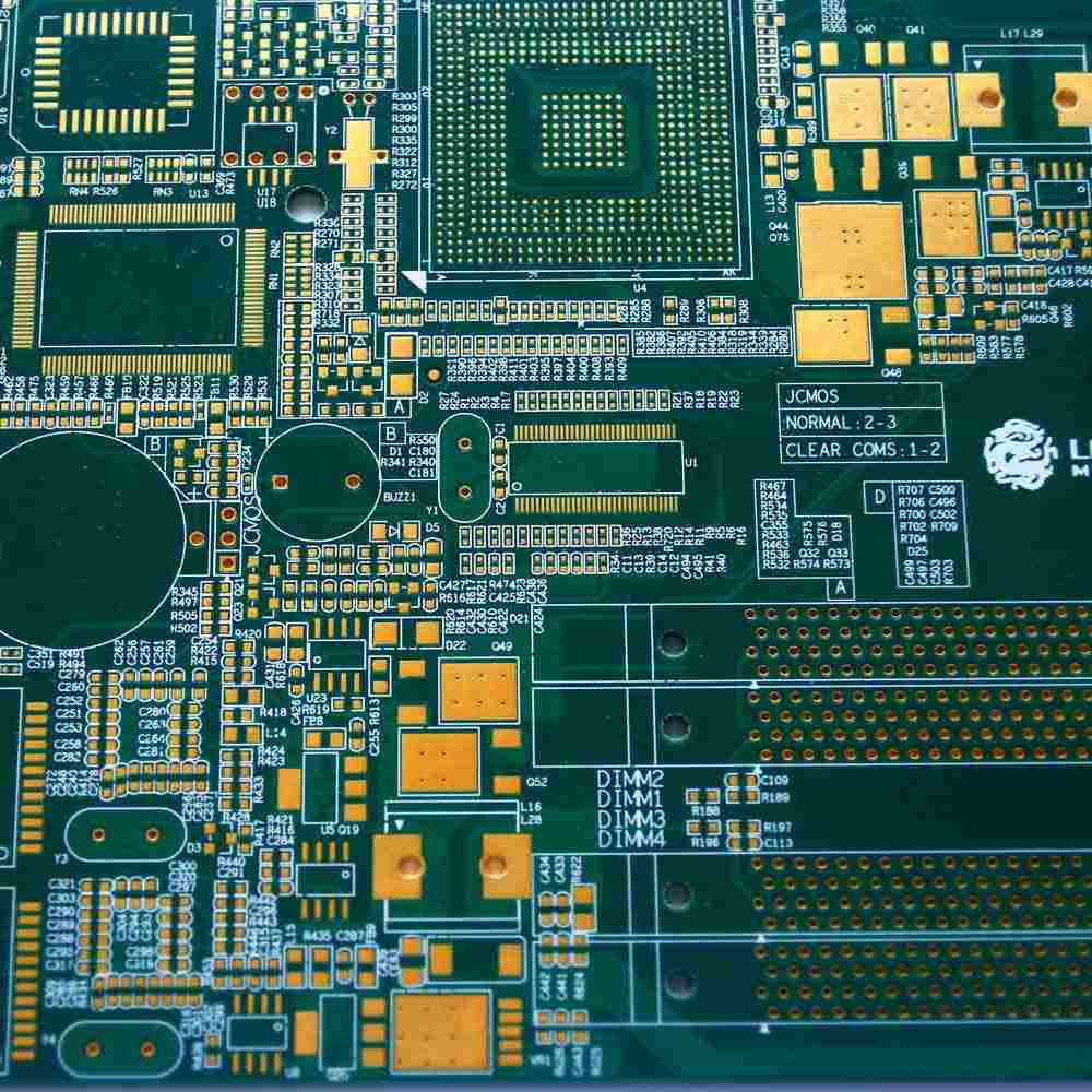
A multi layer PCB consists of three or more conductive copper layers separated by insulating dielectric material. The layers are laminated together under heat and pressure. Multi layer boards allow for greater component density, shorter trace lengths, reduced noise, and improved power distribution compared to single or double sided boards.
Some key terms:
- Layers – The number of copper layers in the PCB. More layers allow for more complex routing.
- Stackup – The sequence and thickness of all materials in the PCB including copper, dielectric, etc.
- Via – A plated through hole connecting traces between layers.
- Blind/Buried Vias – Vias that connect inner layers without going through the entire PCB stackup.
- Impedance Control – Maintaining consistent trace impedance through layer stackup and trace dimensions. Critical for high speed design.
- High Density Interconnect (HDI) – Boards with trace/space under 6 mils, microvias, and often >6 layers.
Key Factors in Choosing a Multi Layer PCB Manufacturer
Here are the top criteria to evaluate when selecting a multi layer PCB fabrication partner:
Capabilities
- Number of layers – Some shops max out at 6 or 8 layers, while others can produce designs with 20+ layers.
- Stackup options – Having a variety of dielectric materials and thicknesses to choose from is important.
- Trace/Space – The smallest trace width and spacing between traces the shop can produce. 6 mils or under is preferred.
- Via types – Support for microvias, blind/buried vias, and stacked vias.
- Impedance control – Ability to precisely match specified trace impedance based on stackup.
- HDI technology – For high density multi layer boards, ensure the shop has advanced HDI capabilities.
- Materials – Variety of dielectric, copper, and finishing options. FR-4, Rogers, Isola, metal core, etc.
- Lead time – Choose a shop with lead times acceptable for your project schedule.
Quality
- Consistency – Repeatable processes and quality across all orders.
- Attention to detail – Careful review of customer designs and requirements.
- Qualifications – Credentials like ISO 9001, IPC Class 3 shop, ITAR registration, etc.
- Testing and inspection – Full testing of bare PCBs as well as automated optical inspection and other quality control checks.
- Yield – Historical fabrication yield rate should be over 95%. Lower rates indicate potential quality issues.
Customer Service
- Communication – Clear and responsive communication during the design, quoting, fabrication, and shipping process.
- Engineering support – Help with DFM, stackup recommendations, and other technical guidance.
- Documentation – Detailed drawings, test reports, CoCs, and other documentation.
- Problem resolution – Quickly investigate and resolve any issues that arise. Offer compensation for defective orders.
Cost
- Pricing structure – Some shops charge by number of layers, others by board area. Understand their model.
- Volume discounts – Offer discounts on larger orders to reduce cost.
- NRE charges – Some shops waive NRE fees for qualified orders.
- Special offers – Sales, promotions, and coupon codes can provide additional cost savings.
Delivery and Logistics
- Shipping options – Offer a choice of shipping methods to meet different delivery timelines.
- Packaging – Boards should be securely packed to prevent damage during shipment.
- Customs expertise – Streamlined processes for international orders including customs documentation.
Top Multi Layer PCB Manufacturers

Here are five leading multi layer PCB manufacturers to consider across a range of capabilities and budgets:
Advanced Circuits
- Location: Aurora, CO
- Capabilities: Up to 32 layers, 4 mil trace/space, microvias, HDI, impedance control.
- Quality: ISO 9001, IPC 6012 Class 3, ITAR
- Cost: Low NRE, competitive pricing, free DFM analysis
- Lead Time: 24-48 hours for prototyping/small runs
Advanced Circuits is one of the fastest PCB shops in the industry. Their “same day” service is ideal for prototyping multi layer boards urgently. They also offer medium to high volume production. Their online quoting and ordering makes procurement easy.
Sierra Circuits
- Location: Sunnyvale, CA
- Capabilities: Up to 30 layers, flex/rigid-flex PCBs, controlled impedance
- Quality: ISO 9001, IPC 6012 Class 3, ITAR
- Cost: Low cost prototype deals (e.g. $33 for 2 layer board in 3 days)
- Lead time: As fast as 24 hours. Standard lead times 5-8 days.
Sierra offers fast turnaround on multi layer prototyping and short runs at very competitive pricing. Their online capabilities make it simple to upload designs, get quotes, and order. They have over 30 years of experience manufacturing complex PCBs.
PCBWay
- Location: China with US/EU warehouses
- Capabilities: Up to 36 layers, 4 mil trace/space, HDI, impedance control, flex/rigid-flex
- Quality: ISO 9001, IPC 6012 Class 3
- Cost: Low cost on small volume. High volume discounts.
- Lead Time: 24-72 hours for prototyping
PCBWay has invested heavily in advanced manufacturing capabilities while keeping costs competitive, especially for prototypes and small orders. Their online capabilities make ordering hassle-free.
Sunstone Circuits
- Location: Mulino, OR
- Capabilities: Up to 48 layers, controlled impedance, flex/rigid-flex
- Quality: ISO 9001, IPC 6012 Class 3, ITAR, ISO 13485 (medical)
- Cost: Instant online quotes. Wide range of volume discounts.
- Lead Time: 48 hours-6 days depending on order complexity
Sunstone focuses on high-mix, low-medium volume orders. Their automated quoting, ordering, and tracking systems help streamline the procurement process. Their advanced capabilities can handle very complex, high layer count designs.
TTM Technologies
- Location: Global facilities in Asia and North America
- Capabilities: 100+ layer PCBs, 3 mil trace/space, Any-layer HDI
- Quality: ISO 9001, IPC 6012 Class 3, AS9100, NADCAP
- Cost: High volume optimized. Very large board size capability.
- Lead Time: Depends on order complexity. As fast as 24-48 hrs.
TTM Technologies is one of the largest PCB manufacturers globally. They specialize in highly complex, advanced technology boards thanks to their cutting-edge fabrication capabilities and scale.
Comparison Table
Here is a comparison of some key capabilities across the top multi layer PCB manufacturers:
| Manufacturer | Max Layers | Min Trace/Space | Impedance Control | Lead Time |
|---|---|---|---|---|
| Advanced Circuits | 32 | 4 mil | Yes | 24-48 hours |
| Sierra Circuits | 30 | 4 mil | Yes | 24 hours+ |
| PCBWay | 36 | 4 mil | Yes | 24-72 hours |
| Sunstone Circuits | 48 | 5 mil | Yes | 48 hours-6 days |
| TTM Technologies | 100+ | 3 mil | Yes | 24-48 hours+ |
The PCB Design and Fabrication Process
Here are the typical steps to take your design from concept through fabrication and assembly when partnering with a multi layer PCB manufacturer:
- Design – Create schematics and layout using EDA software like Altium, Cadence, or OrCAD. Ensure manufacturability with DFM guidelines.
- Quote – Upload your design files to get an instant online quotation from manufacturers. Adjust design as needed based on feedback.
- Fabrication – Place order and your selected PCB shop will fabricate the bare boards per your requirements.
- Testing – Manufacturer tests bare PCBs per IPC standards and sends electrical test reports.
- SMT Assembly – If needed, choose an assembly partner to populate your boards with components.
- Inspection – Manufacturer performs optical and x-ray inspection of assembled boards.
- Shipping – Boards are shipped via your chosen method (FedEx, DHL, etc).
- Integration & Test – You receive, inspect, and test boards before integration into your product.
Tips for a Successful Multi Layer PCB Project
Follow these design, documentation, and procurement tips to ensure your next multi layer PCB project goes smoothly:
- Work closely with your manufacturer’s engineers during design to avoid manufacturability issues. Request their DFM guidelines.
- Clearly define all stackup, layer sequence, material, and impedance requirements in fabrication drawings.
- Confirm your manufacturer has capabilities to meet all trace/space, hole size, and high speed design requirements.
- Provide comprehensive fabrication and assembly drawings with complete notes, dimensions, bill of materials, etc.
- Reviewmanufacturer’s quality certifications and only work with highly qualified shops.
- Build in schedule contingency when possible in case of unexpected delays or defects.
- Carefully inspect boards and test electrically once received before integration.
- Document any issues and work constructively with your manufacturer to resolve them.
Frequently Asked Questions
What are the main benefits of using a multi layer PCB?
Multi layer boards provide higher component density, improved electrical performance through shorter traces, reduced noise through signal isolation, better power distribution, and overall more reliable and compact design versus single or double layer boards. The main tradeoffs are increased cost and complexity.
How many layers do I need for my application?
Most designs can be implemented with 6 layers or less. More complex or high speed designs may require 8-12 layers. Extremely advanced systems can use 20+ layers. Work with your PCB partner to determine the optimal layer count based on your requirements.
What design software do I need for multi layer boards?
Altium Designer, Cadence Allegro, and OrCAD are among the leading professional PCB design suites capable of easily handling the most complex multi layer designs. For simpler boards, Eagle CAD is popular and lower cost.
Can I get impedance control and high speed traces on inner layers?
Yes, precise impedance control of traces on inner layers is possible by carefully controlling dielectric materials, thicknesses, and trace dimensions. Work closely with your fabricator on stackup design.
How much does it cost to add more layers?
While costs vary between manufacturers, typically each additional internal layer adds 15-35% more to the PCB fabrication cost, with more complex stacks at the higher end. Going above 8 layers can get quite expensive.
Conclusion
Multi layer PCBs enable complex, high performance, and reliable electronics design in a compact form factor. Partnering with the right manufacturer is crucial to meet your cost, lead time, quality and capability needs. Do your diligence in evaluating PCB partners, utilize their engineering expertise, and follow sound design practices. This will lead to successful procurement of advanced multi layer circuit boards that exceed performance requirements.


Leave a Reply