Introduction
Printed circuit boards (PCBs) are the foundation of modern electronics, providing the platform to mount and interconnect electronic components. As electronic devices become more complex and compact, PCBs must evolve to accommodate higher density component packaging and interconnect. One technology that has enabled continued PCB evolution is the microvia – a small plated-thru hole that connects adjacent layers in a multilayer PCB stackup. Microvias allow routing connections between layers that would otherwise be inaccessible with standard through-hole vias. This article will provide an in-depth look at microvia technology, its benefits and applications, design considerations, and future outlook.
What are Microvias?
Microvias, as the name suggests, are simply miniature versions of traditional plated through-hole vias with smaller diameters and capture pads. While industry standards do not specify an exact size threshold, microvias are generally defined as vias with diameters under 150μm (or 6 mils). For comparison, standard vias are typically 200μm or larger.
The most common microvia diameter range used today is 50-100μm (2-4 mils), though diameters down to 25μm are possible with advanced processes. Microvias enable connections between adjacent layers in high density interconnect (HDI) PCBs with tight laser-drilled spaces between traces.
Show Image<p style=”text-align:center”> <i>Microvia cross-section – Image source: Morgan Advanced Materials</i></p>
The key differences between microvias and standard vias:
- Smaller diameters – The defining characteristic, enabling high-density routing
- Shorter depths – Microvias only span adjacent layers, not the full PCB stackup
- Thinner capture pads – Reduced capture pad dimensions fit within tight spaces
Benefits and Applications of Microvias
Microvias offer several advantages that have made them essential in advanced PCBs:
High-Density Interconnects
The small footprint of microvias allows routing connections in tight spaces not practical with standard vias. This facilitates complex routing in multi-layer boards.
Layer Count Reduction
By spanning adjacent layers, microvias reduce the number of laminated dielectric/foil layers required to route connections in a PCB stackup.
Component Package Miniaturization
Microvias support the transition to smaller component packages such as QFNs and 0201 discretes that could not be efficiently routed without HDI capabilities.
Increased Routing Channels Microvias multiply the number of vertical routing channels between layers in a PCB stackup.
Improved Signal Integrity
Shorter drilling depths result in reduced inductance for better high-speed signal performance.
Reduced Skew Matching microvia depths between differential pairs lowers skew.
Lower Costs Fewer layers and smaller board sizes reduce costs.
Microvias target high complexity and performance applications such as:
- Smartphones, tablets, and wearables
- High-speed digital circuits
- FPGAs, ASICs, and other IC packages with fine pitch I/O
- HDI PCBs in general
Microvia Design Considerations
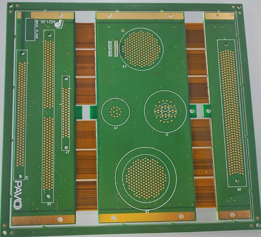
While microvias provide significant benefits, they also impose some design constraints:
Via Reliability The primary reliability concern is potential cracks originating from the thin copper along the microvia barrel. Good process control of plating quality and Tg optimization are key.
Capture Pad Size Small capture pads are more prone to misregistration and tombstoning. Recommended capture pads are 0.2mm larger than the drill diameter.
Stackup Materials Low Tg, high performance dielectric materials may be required to withstand lead-free soldering temps.
Annular Ring A 0.1mm annular ring is recommended for drill-to-capture pad alignment.
Hole Wall Tolerances
Laser drilling process can produce thicker hole walls than mechanical drilling. Factor in adequate capture pad sizing.
Spacing Rules Follow spacing rules between microvias as well as adjacent traces. Consult your fabricator.
Via Fills Copper paste or epoxy ink via fill may be used to plug microvias if reliability is a concern.
With careful design practices, microvias can be implemented successfully on even the most challenging PCBs.
Microvia PCB Fabrication Process
There are two common methods used to manufacture microvias – sequentially laminated and laser drilled build-up.
Sequential Lamination
In this process, alternating layers of dielectric prepreg and copper foil are laminated together to build up the PCB layer by layer. Laser microvias are drilled to interconnect layers after each lamination step. This allows an essentially unlimited number of microvia interconnect layers. However, the multiple lamination cycles increase process complexity.
Laser Drilled Build-Up
Only a minimal circuit board core is laminated initially. Dielectric and copper layers are then built up sequentially using electroless and electrolytic copper plating coupled with photolithographic patterning. Microvias are laser drilled and plated to interconnect layers. While limited in total number of build-up layers, this method simplifies processing.
Both methods produce high quality and can support microvias down to 25μm in diameter or below. Significant investments in laser drilling equipment and cleanroom facilities are required either way.
The Future of Microvias
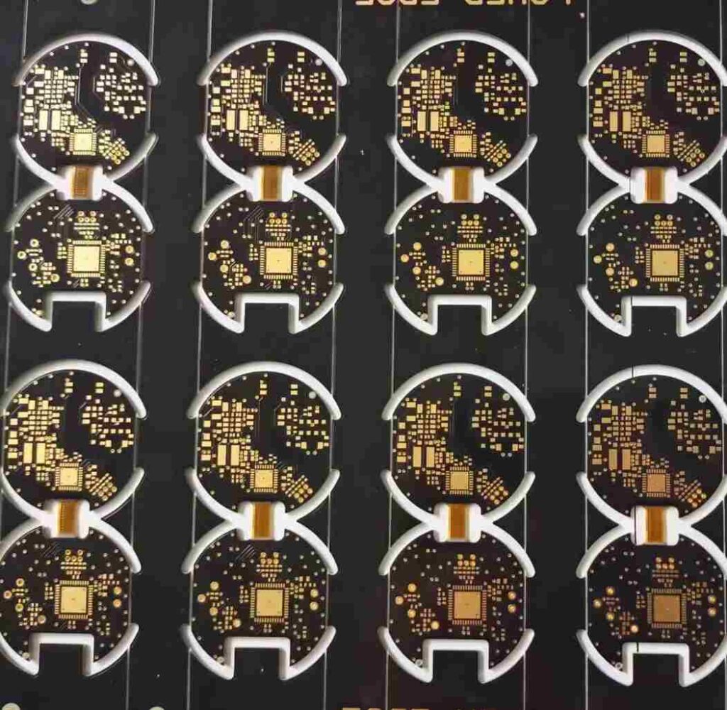
There are ongoing technology developments to enable smaller microvias to meet increasing interconnect density requirements:
- Finer laser drilling – UV and picosecond lasers can drill smaller, higher quality holes
- Improved plating processes – Optimized copper plating baths and profiles for thinner deposits in fine holes
- Novel organic dielectrics – Materials with lower cure temps and loss to further improve electrical performance
- Aluminum usage – Lower resistance aluminum conductors replace copper for some microvia applications
- Guide plate technology – Electroplating guides help plate smaller blind microvias
Microvia technology will continue advancing hand-in-hand with electronic packaging innovations to fuel more powerful and compact designs.
Frequently Asked Questions
Here are answers to some common questions about microvias:
What are the smallest microvia diameters currently produced?
The current lower limit is around 25μm, though some reports indicate specialized processes reaching 20μm diameters. The majority of high volume production remains above 50μm.
Do microvias reduce PCB reliability?
Designed properly, microvia reliability can match or exceed standard plated through holes. The primary reliability concern is potential cracking due to thin copper barrel plating. Proper process control and design practices mitigate these risks.
Can microvias be completely plugged?
Selective copper plating or solder masks may partially plug microvias. Some specialty additives allow complete hole filling, though these can impact soldering. Filled vias are more resistant to cracking and moisture ingress.
Why is laser drilling used instead of other methods?
Laser drilling provides the fine diameter capability and high aspect ratios needed for microvias in multilayer boards. Mechanical drilling cannot presently reach these dimensions reliably.
Are stacked microvias between multiple layers allowed?
Stacked microvias spanning more than two adjacent layers are typically avoided. The long cascaded thermal stresses can lead to reliability issues over thermal cycling.

Leave a Reply