Introduction
High-density interconnect (HDI) printed circuit boards (PCBs) have become increasingly popular in modern electronics due to the demand for miniaturization and high functionality. A key process in manufacturing HDI PCBs is creating microvias – small holes that allow connections between different layers of the board. Traditional mechanical drilling methods have limitations in drilling these tiny vias, which has led to the rise of laser drilling as an alternative.
Laser drilling uses focused laser beams to ablate material and create vias in HDI PCBs. This article will provide an overview of laser drill technology, including the types of lasers used, drilling techniques, and the benefits and challenges of laser drilling for HDI PCBs.
Types of Lasers for Drilling HDI PCBs
Several types of lasers are used for drilling microvias in HDI PCBs:
CO2 Lasers
- Most common laser type used
- Infrared laser with wavelengths around 10 μm
- Can drill vias down to 50 μm in diameter
- Relatively low cost
- Drawbacks are lower precision and slower process compared to other lasers
Nd:YAG Lasers
- Near infrared solid state laser with 1.06 μm wavelength
- Provides good balance of speed, precision, and cost
- Can drill vias around 25-50 μm diameter
- More expensive than CO2 lasers
UV Lasers
- Ultraviolet lasers with wavelengths below 400 nm
- Includes frequency tripled and quadrupled Nd:YAG lasers
- Allows drilling of vias down to 15 μm diameter
- Very precise but much higher cost
Excimer Lasers
- Pulsed ultraviolet gas lasers using reactive gases
- Wavelengths of 193 nm and 248 nm
- Capable of drilling vias down to 10 μm diameter
- Most expensive laser type
Laser Drilling Techniques
There are two main techniques used for laser drilling of HDI PCBs:
Single Shot Drilling
- A single laser pulse is used to drill each via
- Simpler process but diameter consistency can vary
- Usually used for larger vias (>50 μm)
- CO2 lasers most common
Percussion Drilling
- Multiple laser pulses strike the same via location
- Allows drilling of smaller vias with better consistency
- More complex process requiring precise positioning
- Used for microvias below 50 μm diameter
- Nd:YAG or UV lasers preferred
Other advanced techniques like trepanning can also improve hole circularity and precision.
Benefits of Laser Drilling for HDI PCBs
Laser drilling provides several important benefits for manufacturing HDI PCBs:
- Small via sizes – Laser can drill extremely small vias not feasible with mechanical drilling, enabling denser designs.
- High precision – Laser beams can be focused down to micron scales for precision drilling location and shape.
- Non-contact process – No mechanical force applied that could damage fragile boards.
- Fast processing – Lasers can drill vias much faster than mechanical drilling.
- Minimal burring – Laser ablation produces little debris or burring around the via.
- Versatile materials – Effective on a wide range of rigid and flexible PCB materials.
Challenges of Laser Drilling
However, there are also some challenges associated with implementing laser drilling:
- Via taper – Vias can exhibit some taper from laser entrance to exit.
- Thermal damage – Heat can induce microcracks or charring around the via.
- Debris – Ablation produces debris that must be cleaned.
- Complexity – Requires sophisticated laser systems and control.
- Cost – Laser systems have high capital and maintenance costs.
- Safety – Extreme caution required when working with powerful lasers.
Optimizing Laser Drilling Parameters
To achieve good quality microvias, laser drilling parameters must be carefully optimized:
Laser Settings
- Wavelength
- Pulse energy
- Pulse duration
- Pulse frequency
- Shot number
Board Properties
- Material composition
- Thickness
- Target via size
Process Factors
- Beam focusing
- Shot pattern
- Depth control
- Debris removal
- Cooling
Poor parameter selection can lead to issues like incomplete drilling, overheating damage, or poor hole shape. Extensive process development is usually needed to define the ideal laser drilling recipe.
Quality Control for Laser Drilled Vias
Strict quality control is required to ensure vias meet specifications after laser drilling. Common checks include:
- Diameter – Measure via size and circularity with optical or SEM tools.
- Taper – Inspect taper uniformity from entry to exit.
- Location accuracy – Check alignment to pads and layers.
- Wall quality – Evaluate cracking, charring, debris under microscope.
- Cross-section – Cross-section vias to directly examine wall defects.
Automated vision systems are often used for fast and consistent inspection of via geometries. Statistical process control tracks performance over time.
Typical Machine Configuration
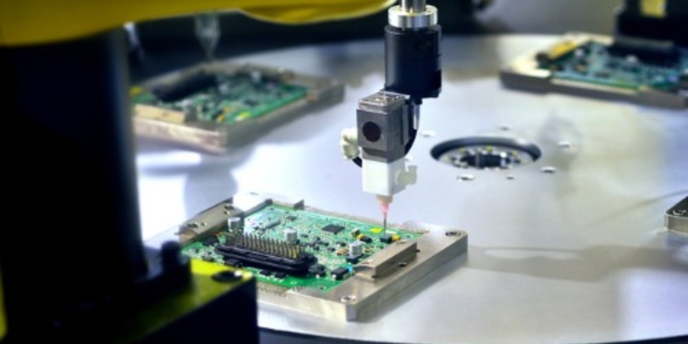
Laser drilling systems require numerous components for smooth and precise operation:
- Laser source – CO2, Nd:YAG, excimer etc matched to target via size.
- Beam delivery – Optics to condition, steer, and focus beam.
- Motion stages – High precision XY stages to position boards.
- Depth control – Methods to detect and control hole depth.
- Debris removal – Air knife, vacuum, or brushes to clean debris.
- Cooling system – Chiller to prevent thermal damage.
- Loading/unloading – Automated mechanisms to load and remove boards.
- Vision system – Cameras for alignment and inspection.
- Computer – Software to program, control, and monitor process.
Recent Developments
Some recent advancements in laser drilling technology for HDI PCBs include:
- Hybrid laser techniques combining different laser wavelengths.
- Specialized beam shaping methods.
- Picosecond and femtosecond lasers for high precision.
- On-the-fly drilling of moving boards.
- Advanced monitoring systems like acoustic sensors.
- Improved automated debris removal strategies.
- Machine learning for smarter process control.
Continued innovations in laser technology, software, and integration will further enhance the capabilities of laser drilling systems for HDI PCB production.
Conclusion
Laser drill technology has become indispensable for manufacturing the microvias required in high density PCB designs. By allowing extremely small via sizes with high precision, lasers enable continuing miniaturization and performance trends in electronics. With different laser types and drilling techniques available, manufacturers can select systems tailored for their specific HDI drilling needs. However, careful process control is crucial to achieve consistent and high quality laser drilled vias. Ongoing advances provide opportunities to further improve the laser drilling process as HDI PCBs become increasingly prevalent.
Frequently Asked Questions
Q: What are the smallest via sizes that can be laser drilled in HDI PCBs?
A: Using ultrafast UV lasers and techniques like percussion drilling, laser systems can drill microvias down to around 10-15 microns in diameter in HDI boards. The thinnest mechanical drilling can typically achieve is around 50 microns.
Q: Does laser drilling work for flexible HDI PCBs?
A: Yes, laser drilling is very effective for flexible PCBs using polymer materials like polyimide. The laser ablates the polymer cleanly without mechanical stress on the thin flexible boards.
Q: Can the same laser drill different via sizes?
A: Generally separate laser systems are used for different via size ranges, but it is possible to drill different sizes on one machine by changing parameters like beam focusing and shot pattern. The range of achievable sizes is limited for a given laser.
Q: Is laser drilling faster than mechanical drilling?
A: Laser drilling can be significantly faster, especially for microvias. Mechanical drilling speed is limited by bit size and rotation rate, while laser pulses can ablate material extremely quickly. However, total throughput depends on handling time between drilling cycles.
Q: Does laser drilling produce rough via walls?
A: Good quality laser drilling can produce very smooth via walls, superior to mechanical drilling. However, improper parameters can result in microcracks or debris roughening the walls. Proper technique is important for clean, cylindrical vias.
Leave a Reply