Introduction
High Density Interconnect (HDI) boards refer to printed circuit boards (PCBs) with a higher wiring density than traditional PCBs. They enable packing of more components in a given area by employing laser drilled microvias to connect different layers in the board. The lamination process and choice of materials are critical to the manufacturing and performance of HDI boards. In this comprehensive guide, we will explore various aspects of lamination and materials selection for optimal HDI boards.
Lamination Process
The lamination process merges all the conductive and dielectric layers to form a multilayer HDI board. It involves applying heat and pressure to fuse the layers together. The key steps are:
Surface Preparation
The individual layers consisting of copper foils and dielectric prepregs undergo surface treatment to enhance bonding. This includes processes like reducing surface oxides and applying chemical treatments.
Layup
The treated foils and prepregs are precisely aligned and stacked up in a layup press to form a laminate stack. Registration accuracy is critical.
Lamination
The laminate stack is subjected to high temperature and pressure in a lamination press. Typical conditions are 180-200°C at 200-300 psi for over an hour. This cures the resin and fuses layers together.
Cooling and Trimming
After lamination, the HDI board is slowly cooled to prevent warpage. It is trimmed to remove excess material.
Post Lamination Processes
Additional steps like microvia drilling, metallization, and testing are done post-lamination to complete HDI board fabrication.
Proper lamination is key to avoiding defects like layer separation, registration issues, and warpage. Parameters like temperature, pressure profiles, flatness must be tightly controlled.
Core Materials
The core or base laminate material forms the foundational layer in an HDI board. Key requirements for HDI board cores:
- Dimensional Stability: Low coefficient of thermal expansion for reliability during lamination and assembly.
- High Glass Transition Temperature: Withstands HDI lamination temperatures of 180°C or more.
- Low Loss: Low dielectric constant and loss tangent for better electrical performance.
- Smooth Copper Bonding: Good adhesion to copper foils during lamination.
- Laser Drillability: Clean ablation when drilling microscopic vias with lasers.
Some common materials used are:
| Material | Description |
|---|---|
| FR-4 | Glass reinforced epoxy. Low cost but higher losses. |
| Polyimides | High temperature resistance but more expensive. Eg. ULTEM, Arlon 85N. |
| PTFE Composites | Modified with ceramic fillers for better performance. Eg. Rogers RO4350B. |
| LCP | Liquid crystal polymer. Extremely stable but costly. |
The choice depends on electrical, thermal, and drilling requirements.
Prepreg Materials
Prepreg refers to the resin-impregnated glass fabric used to bond the layers in a multilayer PCB. For HDI boards, prepregs must fulfill:
- Low CTE: Prepregs should have optimized glass styles and fills for better CTE matching with copper and cores. This reduces stresses during lamination.
- High Glass Transition Temperature: Withstand high lamination temperatures.
- Good Dielectric Properties: Low Dk andDf values to prevent signal losses.
- Workable Viscosity: Resin viscosity should promote excellent wetting with foils and cores.
- Clean Laser Drilling: No residue or smudging around microvias.
Materials like 170°C FR-4, polyimide, BT-epoxy, PTFE composites are used. The resin system and glass fabric are tailored for HDI needs.
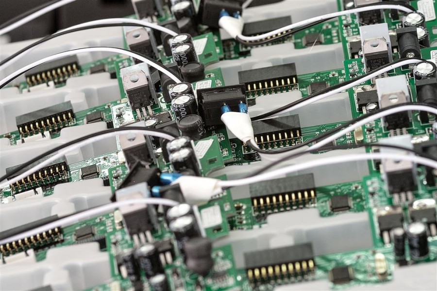
Copper Foil
Copper foils act as the conductive layers in an HDI board. Important characteristics are:
- Thin Foils: Thinner foils down to 3-5μm are used to get finer lines, spaces and high layer counts.
- Surface Treatment: Treatments like RTF (reverse treat foil) improve bond strength during lamination.
- High Elongation: Foils should have over 20% elongation to withstand multilayer lamination stresses.
- Fine Grain Structure: Ensures excellent laser drillability and avoids micro cracks.
Standard ED copper foils are typically used. Some enhanced foils improves yield for ultra-HDI boards.
Solder Masks
The solder mask coats the PCB to control solder spreading and prevent shorts. For HDI boards, key considerations are:
- Resolution Capability: Can achieve fine openings down to 25-50μm or lower.
- Solder Resistance: Withstands reflow temperatures with minimal shrinkage or curing.
- Smooth Finish: Provides a uniform coating, free of defects.
- Laser Ablation: Can be cleanly ablated by lasers when forming openings over microvias.
Photoimageable liquid solder masks that can be exposed with finer details work well. Both UV and thermally cured options are available.
Frequently Asked Questions

Q1. What are some challenges when laminating HDI boards?
Some lamination challenges are:
- Achieving extremely high alignment accuracy between layers. Misregistration can cause shorts or reliability issues.
- Preventing thin core warpage at high temperatures. Warpage leads to problems in via drilling, metallization, and assembly.
- Eliminating lamination induced fractures or separations, especially with thinner copper foils.
- Minimizing resin flow out of stack that can block laser drilled microvias.
Q2. How are very high layer count HDI boards fabricated?
For layer counts above 20 layers, boards are fabricated in separate sections that are eventually bonded together. Some approaches are:
- Sequential Lamination: Building up a thick core with multiple sub-sections containing 4-8 layers each, which are sequentially bonded.
- Parallel Processing: Producing separate high layer count sub-assemblies of up to 10-12 layers each using cluster lamination. These are then aligned and bonded to form a finished board.
- Hybrid Approach: Combining sequential lamination and parallel processing for very high layer counts exceeding 40 layers.
Q3. What are some via drilling guidelines for HDI boards?
Some key HDI board via drilling guidelines:
- Use UV lasers with short wavelengths (355nm, 266nm) for drilling microvias under 75-100μm diameter with good sidewall quality.
- Maintain tight laser energy control to ablate different core, prepreg, and copper materials cleanly without excessive heating.
- Apply venting below microvias and use thin cores to allow escaping decomposition gases during drilling.
- Use low-flare, low-taper drill bits for mechanical drilling to minimize damage in pad areas.
- Keep high spindle speeds above 90,000 rpm and low infeed rates for best accuracy.
Q4. How to minimize warpage in HDI boards?
Methods to reduce warpage in HDI boards:
- Use core and prepreg materials with low, matched CTE to minimize thermal stresses. Synthetic materials perform better than woven glass.
- Keep overall laminate thickness balanced and symmetric by using same materials in similar stack up on both sides of core.
- Allow sufficient dwell time during the high-temperature lamination cycle for viscosity reduction and stress relaxation.
- Optimize cooling after lamination to ensure uniform, controlled cooling without temperature gradients.
- Use balanced metal deposition or apply stress balancing coatings post-lamination to offset metal stresses.
Q5. What are the functions of a solder mask coating?
Key functions of a solder mask coating:
- Protects the underlying board surface from the environment and handling damage.
- Controls solder spreading by defining keep-out areas around pads. This prevents shorts.
- Provides electrical isolation with high surface resistivity.
- Contains reference markings or legends for assembly and inspection.
- Improves soldering performance by promoting wetting on relevant pads and pins.
- Protects board and components from repeated thermal stresses during assembly reflows.
Summary
HDI board fabrication demands careful attention to the lamination process and material selection. A good lamination process fusion bonds the thin dielectric and foil layers effectively to produce a void-free, warp-free board without defects. Suitable core, prepreg, foil and solder mask materials must be chosen for dimensional stability, thermal endurance, electrical performance, and drillability. By following sound design and process guidelines, high quality HDI boards can be manufactured for advanced applications.


Leave a Reply