Introduction
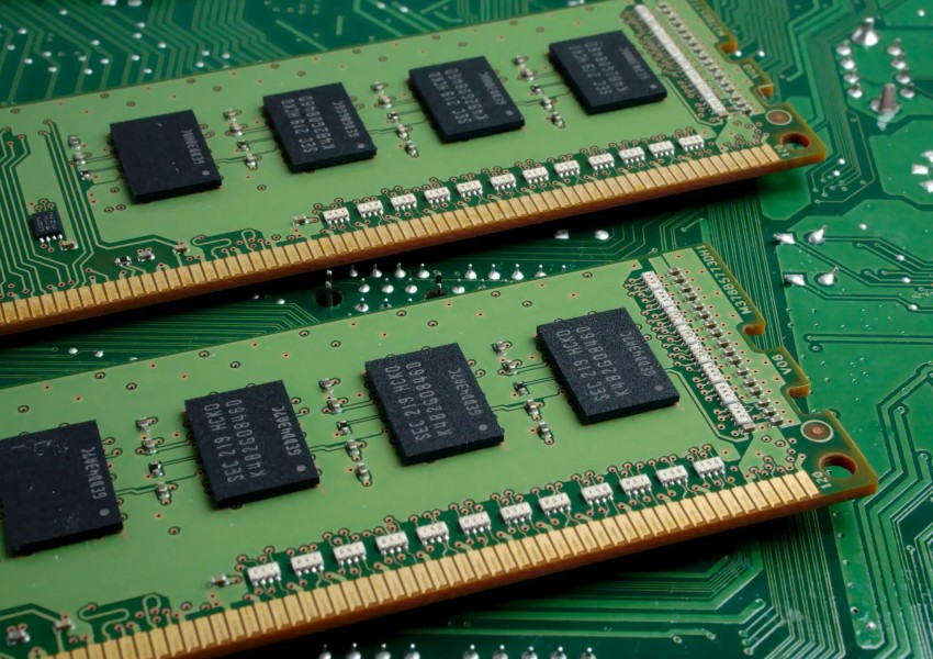
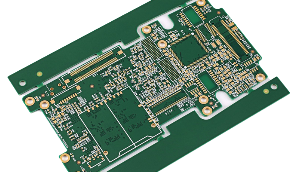
A printed circuit board (PCB) serves as the foundation for almost all modern electronics. It provides the mechanical structure and electrical connections between components. Vias play a critical role in allowing signals and power to be routed between layers in multilayer PCBs. However, there has been some debate around whether vias have detrimental effects on PCB performance and reliability. This article will examine the pros and cons of vias and analyze whether they should be considered “bad” for PCB design.
What is a Via?
A via is a plated through-hole that connects two or more layers in a PCB. Vias allow traces to change layers, connecting components and signals on the top and bottom of the board. There are three main types of vias:
- Through-hole via: Goes through the entire PCB from top to bottom.
- Blind via: Connects an outer layer to an inner layer. Does not go through the whole board.
- Buried via: Connects two or more inner layers without connecting to an outer layer.
Vias are plated with copper to create the electrical connection between layers. They may also be filled with epoxy or other materials to provide structural integrity and prevent solder wicking.
Potential Downsides of Vias
While essential for routing, vias also introduce some potential downsides that must be considered in PCB design. Here are some of the possible disadvantages of using vias:
- Signal integrity: Vias can introduce impedance discontinuities, reflections, and crosstalk that may disrupt sensitive signals. This is especially true at high frequencies.
- Thermal resistance: The hole in the center of a via acts as a thermal barrier. This can cause localized heating if high currents pass through vias.
- Manufacturing defects: It’s possible for vias to develop cracks or separation between layers during manufacturing. This reduces reliability.
- Difficult inspection and repair: It’s harder to inspect and repair vias compared to traces on outer layers. X-ray inspection may be required.
- Increased cost: Adding vias increases drilling time and complexity during PCB fabrication. More vias means higher cost.
Optimizing Via Design
While vias can introduce challenges, following good design practices can mitigate any potential downsides:
- Minimize unnecessary vias: Only use vias where routing requires layer changes. Avoid “via farms”.
- Place vias intelligently: Locate vias away from sensitive components or signals when possible.
- Use thermal relief pads: Add copper pads around vias carrying high currents to reduce localized heating.
- Select optimal drill size: Match via drill size to current levels and manufacturability.
- Plate thoroughly: Ensure vias are plated through fully with no gaps or thinning.
- Perform analysis: Use modeling, simulation, and impedance calculations to optimize via design.
- Conduct testing: Verify via integrity through thermal stress, vibration, and electrical testing.
Table: Via Design Guidelines
| Parameter | Recommendation |
|---|---|
| Via drill size | Match to trace width, 0.3-0.6 mm typical |
| Antipad size | 1.2-1.5x drill size |
| Thermal relief pad | Used for high power vias > 1 A |
| Minimum annular ring | 0.15-0.25 mm |
| Spacing | At least 2x drill size |
| Max aspect ratio | 10:1 (length:diameter) |
Do Vias Impact Signal Integrity?
One of the biggest concerns with vias is their potential impact on signal integrity at high speeds. Vias introduce discontinuities and impedance mismatches that may reflect or distort signals. However, following good design practices can minimize any detrimental effects:
- Match impedances: Make sure traces have matched impedance on all layers connected by a via.
- Place vias carefully: Avoid putting vias in sensitive high-speed signal paths if possible.
- Use backdrilling: Backdrilling eliminates unused via portions to remove impedance discontinuities.
- Minimize stubs: Stubs should be less than 1/10 of a wavelength to avoid resonances.
- Use filled vias: Filling vias with epoxy minimizes impedance variations.
- Simulate performance: Model signals through vias to verify acceptable performance margins.
With careful engineering, vias can often be designed to have minimal impact on signal integrity. Testing and measurement should be used to confirm acceptable performance.
Effect of Vias on EMI and EMC
Vias also have implications for EMI (electromagnetic interference) and EMC (electromagnetic compatibility). A via forms an aperture for electromagnetic radiation that could potentially cause unwanted emissions or couple in external noise. Some key considerations include:
- Shielding: Placing grounded vias around the perimeter of the PCB can form a Faraday cage to contain emissions.
- Spacing: Having a tight spatial distribution of vias helps limit emitted radiation.
- Filling vias: Filling with epoxy minimizes cavities that can resonate and radiate energy.
- Filtering: Adding ferrite beads or other filters on via transitions containing high frequency signals reduces emissions.
- Board stackup: Careful layer stackup and breakout planning minimizes radiation from trace-via transitions.
- Simulation: Model EMI and use analysis tools to predict emissions and susceptibility.
With good EMC engineering practices, vias do not inherently result in unacceptable emissions or immunity problems. Testing should always verify acceptable EMI/EMC performance.
Do Vias Reduce Reliability and Yield?
Another concern is whether vias might reduce the reliability or manufacturing yield of PCBs. Potential factors include:
- Separation or cracking: Thermal stress can cause inner layer separation or cracked plating.
- Voids: Incomplete plating may leave holes and voids within a via.
- Resin recession: The resin around a via might recede during thermal stress.
- Solder wicking: Solder could be drawn up into open vias during assembly.
However, following robust design and fabrication practices minimizes these risks:
- Conservative layout: Avoid minuscule annular rings and high aspect ratio vias.
- Thorough plating: Use direct plating with sufficient overplating thickness.
- Stress relief: Thermal relief pads and filling vias reduces stress.
- Redundant vias: Provide duplicate vias for critical connections.
- Inspection: Automated optical, X-ray and cross-section inspection checks for defects.
- Environmental testing: Thermal cycling, vibration, shock, and power cycling verifies integrity.
While vias were more problematic many years ago, improvements in materials, design tools, and manufacturing techniques have made them quite reliable when properly engineered. Testing provides further assurance of robustness.
Do Vias Increase PCB Fabrication Cost?
It’s certainly true that adding vias increases the drilling time and complexity during PCB fabrication. The fabrication cost per board will go up as the number of vias is increased. However, this does not mean vias should be avoided solely due to cost considerations. Some key points:
- Only eliminate unnecessary vias: Minimizing superfluous vias reduces costs without compromising design.
- Weigh pros/cons: The benefits of vias often outweigh a small cost increase. Evaluate overall system cost.
- Use design rules checks: Tools highlight excessive or redundant vias to remove.
- Combine holes: Gang drilling vias together into panels lowers costs.
- Review stackup: An optimized layer stackup can reduce the number of vias needed.
- Benchmark pricing: Get quotes from multiple fabricators to compare via costs.
The incremental cost increase from properly utilized vias is usually acceptable. Eliminating all vias could require more layers, increasing cost far more. As with any design decision, tradeoffs should be evaluated.
Conclusion
Vias remain an essential element of printed circuit board design, enabling complex multilayer routing. While they can introduce some potential drawbacks, following good engineering practices typically minimizes any negative impacts of vias. Via cost increases are usually acceptable given the design flexibility provided. Overall, vias should not be viewed as “bad” for PCBs. Through appropriate use and optimization, they provide indispensable interconnectivity with acceptable tradeoffs.
Frequently Asked Questions
1. How are vias constructed?
Vias are formed by drilling holes through a PCB substrate and then electroplating the holes to metallize the interior walls. The vias are often filled with epoxy after plating for structural integrity and to prevent solder wicking.
2. What are some alternatives to vias?
Some alternatives to vias include:
- Buried stripline routing layers to avoid layer transitions
- Skipping vias by routing multiple layers to “snake” traces
- Using edge plating or castellated pads for interlayer connections
- Employing wire links or vertical interconnect access (VIA)
However, vias remain the most widely used and cost-effective approach.
3. How do I calculate the size and number of vias needed?
Via size should match the width of the traces being connected, with drill size typically being 0.3-0.6mm. Use sufficient vias to carry the expected current, allowing at least 0.8 A per via. Space vias at least 2x the drill diameter apart. Analyze thermal performance to determine heating.
4. Can vias be repaired if defective?
It is difficult to repair buried vias inside a fabricated PCB. Opens might be bridged by soldering a wire on the surface. Design redundancy provides alternative paths if individual vias fail. Test thoroughly to detect any defects before assembly.
5. What are some key rules for high-speed via design?
Guidelines include matching trace impedances, minimizing stub lengths, using filled vias, providing ground isolation, limiting transitions, simulating performance, and backdrilling unused portions of vias. Careful signal integrity engineering minimizes issues.


Leave a Reply