
Optimizing Interconnects for Signal Integrity and Performance
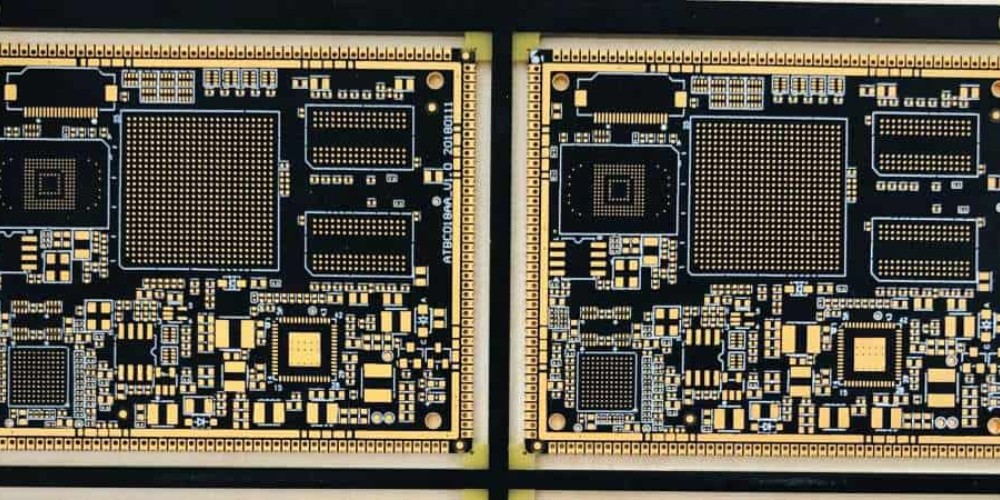
As printed circuit boards (PCBs) increase in complexity, with higher pin counts, faster signal speeds, and tighter spacing, optimizing interconnects becomes critical. Interconnects refer to the traces, vias, and other conductive elements that connect components on a PCB. Proper interconnect design ensures signal integrity, reduces electromagnetic interference (EMI), and enables boards to perform reliably at high frequencies.
There are several key factors to consider when designing interconnects:
Signal Routing
- Minimize trace length
- Use 45° or curved traces instead of 90° turns
- Avoid acute angles that cause impedance discontinuities
- Route differential pairs on same layer with consistent spacing
Stackup Planning
- Dedicate layers for power and ground to isolate signals
- Use thicker copper weights for power distribution
- Place sensitive signals layers next to reference planes
Transmission Line Effects
- Match trace width and spacing to target impedance
- Control impedance throughout path including vias
- Terminate traces to minimize reflections
Cross Talk
- Maintain adequate distance between traces
- Route aggressor signals orthogonal to victim signals
- Use ground guards around sensitive traces
Paying attention to these considerations during layout will minimize loss and distortion and enable high speed, low noise operation.
Modeling and Simulating Interconnects
To verify interconnect performance before manufacturing PCBs, engineers use modeling and simulation software. These tools can accurately predict signal behavior based on physical design attributes. Common analyses include:
- Transient – examines signal waveforms in time domain
- AC analysis – frequency domain simulation
- IBIS – simulate behavior using component models
- Power integrity – confirm clean power delivery
- EMI/EMC – model emissions and susceptibility
Simulation enables engineers to visualize effects like ringing, overshoot, coupling, ground bounce, and reflections. Models can be tuned and the design adjusted until requirements are met. This prevents costly re-spins and speeds time-to-market.
Material Selection for Optimal Performance
In addition to physical design, appropriate materials are needed for a robust interconnect system. Key considerations include:
Dielectrics
- Low loss tangent to minimize signal loss
- Tight dielectric constant (Dk) tolerance for impedance control
- High resin content improves manufacturability
| Material | Dk | Loss Tangent |
|---|---|---|
| FR-4 | 4.5 | 0.02 |
| PTFE | 3.0 | 0.001 |
| Ceramic filled PTFE | 3.5 | 0.003 |
Copper
- Thicker copper reduces resistive losses
- Smooth copper foils limit signal degradation
- Copper weights up to 5 oz./ft2 or more for power planes
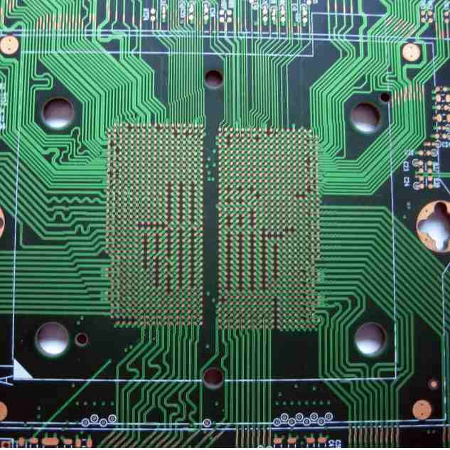
Vias
- Plated through hole vias for reliability
- Microvias for HDI designs
- Filled and capped vias for high frequency boards
Using advanced PCB materials enhances electrical performance and reliability while meeting fabrication requirements.
Interconnect Considerations for High Speed Designs
For multi-gigabit data rates, interconnects must be precision engineered to maintain signal fidelity. Here are key factors to address:
Controlled Impedance transmission lines
- Matched to source, load, and cable impedance
- Consistent dimensions and dielectric constant
- Tolerances within 5%
Layer stacking and arrangement
- Staggered power and ground planes for decoupling
- Reference planes adjacent to signal layers
- judicious use of buried and blind vias
Minimize vias
- Limit transition through via barrel
- Laser drilled microvias
- Extend reference planes through vias
Reduce stubs
- Keep lines short, direct
- Use blind and buried vias
- Eliminate unused pads
Careful modeling, material selection, and PCB fabrication and assembly are essential to achieve multi-gigabit data rates. Attention to good high speed design principles establishes a robust interconnect system.
Interconnect Considerations for RF Boards
Radio frequency (RF) boards which operate at up to millimeter wave frequencies have particular demands:
- Precisely tuned trace dimensions to match waveguide geometry
- Tight thickness and etch control for trace impedance
- Smooth copper and low loss dielectric materials
- Minimize discontinuities and parasitics
- Carefully designed component pads, holes, and keepouts
- Strategic grounding and shielding
Many times copper thickness is increased to 3 oz. or greater to reduce resistive losses at high frequencies. Silver plating may also be used.
Vias can cause problems if not properly designed. Back-drilled or blind vias are used to eliminate via stubs. Carefully tuned via fences around components prevent unwanted coupling while maintaining low inductance grounding.
Reliable RF performance requires specialized modeling techniques coupled with precise PCB fabrication and assembly. Working closely with fabrication partners helps achieve RF objectives.
Summary of Interconnect Design Considerations
To summarize, key elements for optimizing interconnects include:
- Careful routing and layer stack planning
- Extensive modeling and simulation
- Judicious material selection
- Tight process controls and tolerances
- Strategic component layout
- Attention to manufacturability
With increasing demands on PCB performance, interconnects play a pivotal role in overall system reliability. Paying attention to these considerations will ensure the interconnect system meets both signal integrity and manufacturing needs.
FAQ
What are some key factors when routing traces for impedance control?
Some key factors for impedance control when routing traces are:
- Match desired impedance target by setting appropriate trace width/space ratio
- Maintain consistent trace dimensions throughout path
- Route traces over continuous reference plane whenever possible
- Avoid stubs, non-90 degree angles, and impedance discontinuities
- Use matched length differential pairs with controlled skew
- Keep lines short and direct for low loss and reflection control
How can vias negatively impact signal integrity?
Vias can negatively impact signal integrity in several ways:
- Impedance mismatch through via barrel
- Parasitic capacitance to reference planes
- Inductance of via stub if not properly terminated
- Coupling between signals transitioning through common via
- Reflections and resonances if via not properly modeled
- Reliability issues like barrel cracks under thermal stress
What are some methods to reduce EMI from interconnects?
Methods to reduce EMI from interconnects include:
- Enclose traces in continuous ground guard traces or planes
- Route traces orthogonally to reduce coupling
- Use ground vias to break up ground return loops
- Filter connector pins
- Increase spacing between aggressor and victim traces
- Minimize parallels between clocks, data, control lines
- Avoid 90 degree turns; use arcs, curves in traces
- Minimize overall loop areas
How are PCB interconnects modeled for signal integrity analysis?
Interconnects are modeled by representing their physical properties like shape, dimensions, materials using a SPICE type circuit model. Transmission line models are used with parameters like RLCG values, dielectric constant, and loss tangent. Both frequency-dependent and time-domain models can be created for SI analysis.
Why are low-loss materials preferred for high speed interconnects?
Low-loss dielectric materials are preferred because they do not attenuate or distort signals as much. With high data rates, dielectric loss and skin effect can severely degrade signals over a trace length. Low Dk reduces propagation delay while tight tolerance controls impedance. Low loss tangent (Df) reduces attenuation. These improve signal fidelity and allow broader bandwidth.


Leave a Reply