Introduction
Printed circuit boards (PCBs) are an essential component of most electronic devices and equipment. They provide the foundation on which chips, capacitors, resistors and other components are mounted and connected to create functional circuits. While PCBs were traditionally assembled by hand, the growth of electronics manufacturing led to the development of industrial PCB assembly processes to enable high-volume production.
In industrial PCB assembly, components are mounted and soldered onto bare PCBs using automated assembly machines and soldering equipment. This allows electronic products to be assembled quickly, consistently and cost-effectively. Understanding the stages, processes and key considerations of industrial PCB assembly is important for electronics manufacturers looking to optimize their production.
Stages of Industrial PCB Assembly
Industrial PCB assembly generally involves three main stages:
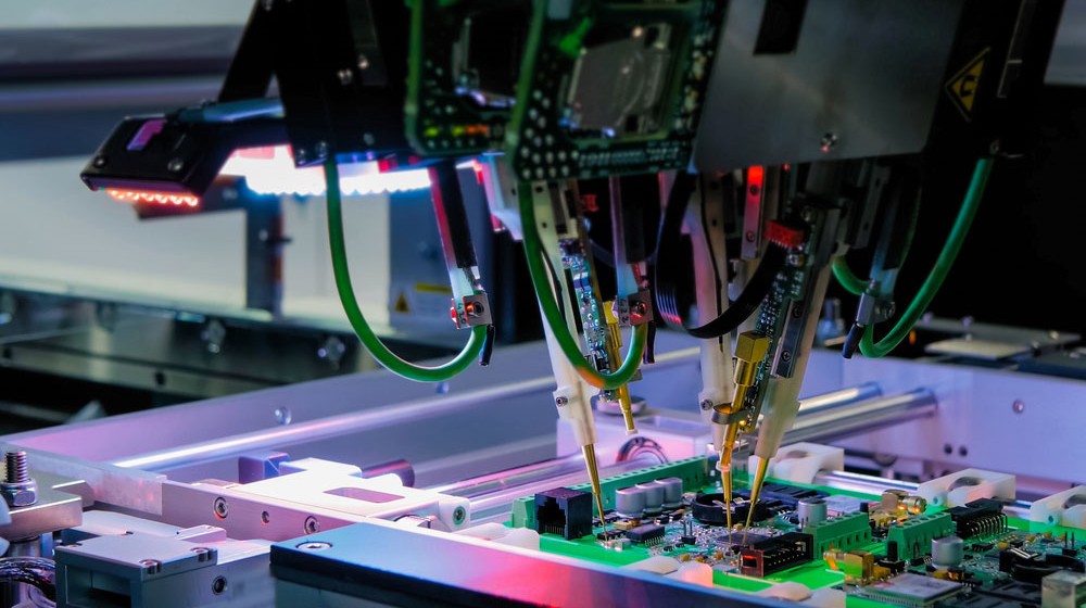
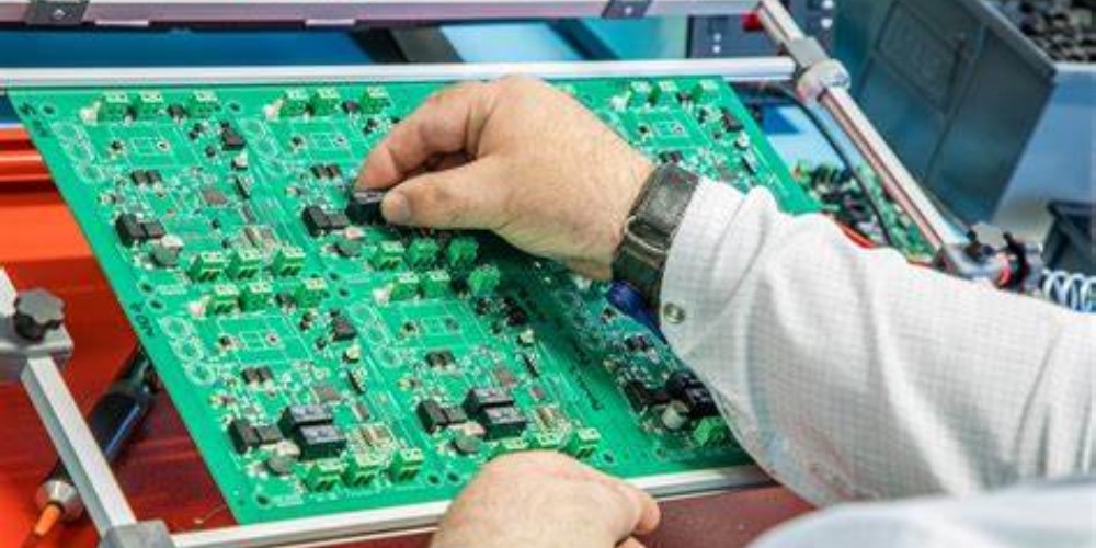
1. Component Placement
This first stage involves mounting and securing components onto the PCB. Some key processes include:
- SMD Placement – Surface mount devices (SMDs) like chips and capacitors are precisely positioned and mounted onto the PCB using pick and place machines.
- Through-Hole Component Insertion – Components with leads like resistors and connectors are inserted into holes drilled in the PCB either manually or using automatic insertion machines.
- Adhesive Application – Adhesives are applied to permanently secure certain components to the board.
2. Soldering
After component placement, the components are soldered to form electrical connections and permanent joints. Common soldering techniques include:
- Reflow Soldering – For soldering SMDs. Solder paste is first applied to PCB pads. The board then passes through a reflow oven to melt the solder and form joints.
- Wave Soldering – For soldering through-hole components. Molten solder waves flow over the bottom of the PCB to fill the plated through-holes.
- Selective Soldering – Uses a soldering iron or nozzle to manually or automatically solder specific joints. Useful for rework or repair.
- Vapor Phase Soldering – An alternative to reflow soldering that uses vapor condensation to evenly heat the PCB.
3. Post-Soldering Processes
After soldering, PCBs undergo additional processes to prepare them for functionality testing and use:
- Cleaning – Removes solder flux residues and other contaminants using cleaning solutions.
- Inspection – PCBs are visually inspected and often go through automated optical inspection (AOI) to check for defects.
- Testing – PCBs are electically tested to validate all connections and ensure boards are functioning properly.
- Conformal Coating – A protective coating applied to shield the PCB from environmental contaiminants.
Key Considerations for Industrial PCB Assembly
There are several important factors to consider when planning your industrial PCB assembly process:
Board Design
- The PCB design must optimize placability and solderability. SMD pads and through-holes should be appropriately sized and spaced.
- Minimize component placement on board edges to avoid issues with pick and place machines.
- Include testpoints to facilitate testing and debugging.
- Design with manufacturability in mind. Seek DFM guidance from your PCB assembly partner.
Component Sourcing
- Source components from trusted suppliers that meet spec requirements.
- Procure reels of SMDs in tape and reel packaging for automated placement.
- Ensure component packages are compatible with assembly equipment at the production facility.
Solder Paste and Solder Mask
- Use solder paste matched to your assembly requirements in terms of alloy type, particle size and viscosity.
- Solder masks define solderable and non-solderable areas. A well-designed mask reduces bridging risks.
Assembly Equipment
- Select equipment suitable for your PCB size, complexity, volume needs and budget.
- Precision pick-and-place machines and optimized component feeders minimize placement defects.
- Reflow ovens and wave soldering machines should deliver even, consistent heat.
Process Control and Optimization
- Use statistical process control (SPC) and tools like control charts to minimize defects and variability.
- Perform regular machine maintenance and calibration for consistent performance.
- Continuously inspect processes and implement improvements through kaizen events.
Conclusion
Industrial PCB assembly enables the mass production of electronic products through optimized automated processes. While the assembly stages of component placement, soldering, cleaning and testing may seem straightforward, careful planning and preparation is required to execute high-yield assembly at scale. Working closely with an experienced PCB assembly partner right from the design stage and leveraging their process capabilities is key to achieving assembly excellence and product quality.
Frequently Asked Questions
Q: What are the benefits of industrial PCB assembly vs. manual assembly?
A: Industrial PCB assembly offers much higher throughput and consistency compared to manual assembly. Automated machines can place tens of thousands of components per hour with precision. This allows large volumes of PCBs to be assembled quickly and cost-effectively.
Q: What types of components can be used in industrial PCB assembly?
A: Common component types assembled include surface mount devices (SMDs) like resistors, capacitors and ICs as well as through-hole components like connectors. Hybrid assemblies with both SMDs and through-hole components are also common.
Q: How are very small SMD components handled in assembly?
A: Extremely small chip components (0201 size and smaller) can be challenging for standard pick and place machines. Specialized high precision placers are used for assembling these micro components. The PCB design should also provide sufficient space around the pads.
Q: Can PCB assembly be fully automated?
A: While processes like SMD placement and soldering are automated, some manual operations are still required for setup, changeover, visual inspection and touch-up work. Fully lights-out assembly lines are still not common. Human oversight remains important for quality and flexibility.
Q: How are design and assembly considerations aligned?
A: To avoid assembly issues, the PCB design should be optimized keeping manufacturability in mind through design-for-manufacturing (DFM) practices. Close designer-assembler collaboration right from the start of the design process is highly recommended.


Leave a Reply