What is PCB Soldermask?
PCB soldermask, also known as solder resist or solder mask, is a protective layer applied to the copper traces of a printed circuit board (PCB) to prevent solder from bridging between conductors during the soldering process. It also provides insulation and protection against oxidation and environmental contaminants.
Soldermask is typically a polymer-based ink that is applied to the PCB surface through screen printing or photoimaging techniques. The most common soldermask colors are green, red, blue, and black, although other colors are available for specific applications or aesthetic purposes.
Functions of PCB Soldermask
- Prevents solder bridges: Soldermask acts as a barrier between adjacent copper traces, preventing solder from accidentally connecting them during the soldering process.
- Insulation: The soldermask layer provides electrical insulation between the copper traces and components, reducing the risk of short circuits.
- Protection against oxidation: Soldermask protects the copper traces from oxidation and corrosion, which can degrade the PCB’s performance and reliability over time.
- Environmental protection: The soldermask layer also shields the PCB from environmental contaminants such as moisture, dust, and chemicals.
- Improved aesthetics: Soldermask gives the PCB a clean, professional appearance and can be used to add branding or labeling to the board.
Why is Testing PCB Soldermask Important?
Testing PCB soldermask is crucial to ensure the quality, reliability, and longevity of the printed circuit board. Some of the key reasons for testing soldermask include:
- Identifying defects: Testing helps identify any defects in the soldermask layer, such as pinholes, cracks, or inconsistent coverage, which can compromise the PCB’s performance and reliability.
- Ensuring proper adhesion: Soldermask must adhere properly to the PCB surface to provide effective protection. Testing can verify the adhesion strength between the soldermask and the PCB substrate.
- Confirming insulation properties: Testing can confirm that the soldermask provides adequate electrical insulation between the copper traces and components.
- Meeting industry standards: Many industries have specific standards and requirements for PCB soldermask performance. Testing ensures that the PCB meets these standards, such as IPC-SM-840 or IPC-A-610.
- Preventing costly failures: Identifying and addressing soldermask issues early in the manufacturing process can prevent costly failures and product recalls down the line.
Methods for Testing PCB Soldermask
There are several methods for testing PCB soldermask, each designed to evaluate different aspects of the soldermask’s performance and quality. Some of the most common testing methods include:
1. Visual Inspection
Visual inspection is the most basic form of PCB soldermask testing and is typically performed throughout the manufacturing process. This method involves examining the PCB surface under magnification to identify any visible defects or inconsistencies in the soldermask layer.
Common issues that can be detected through visual inspection include:
- Pinholes or voids in the soldermask
- Cracks or peeling of the soldermask
- Inconsistent soldermask coverage
- Contamination or foreign materials on the soldermask surface
- Misaligned or incomplete soldermask openings
While visual inspection is a simple and cost-effective method, it is limited by the inspector’s skill and the magnification level used. More advanced testing methods are often necessary to detect subtle or hidden defects.
2. Thickness Measurement
Measuring the thickness of the soldermask layer is important to ensure that it provides adequate insulation and protection for the PCB. Insufficient Soldermask Thickness can lead to reduced insulation properties and increased susceptibility to damage, while excessive thickness can cause issues with component placement and solderability.
There are several methods for measuring soldermask thickness, including:
- Micrometer measurement: A digital or mechanical micrometer can be used to measure the thickness of the soldermask layer at specific points on the PCB. This method is simple but may not provide a complete picture of the soldermask thickness across the entire board.
- Cross-sectional analysis: A cross-section of the PCB can be prepared and examined under a microscope to measure the soldermask thickness. This method provides a more accurate representation of the soldermask thickness but is destructive and time-consuming.
- Eddy current testing: This non-destructive method uses electromagnetic induction to measure the soldermask thickness. An eddy current probe is placed on the PCB surface, and the soldermask thickness is determined based on the probe’s electrical impedance.
| Method | Advantages | Disadvantages |
|---|---|---|
| Micrometer measurement | Simple, non-destructive | May not provide a complete picture of soldermask thickness |
| Cross-sectional analysis | Accurate representation of thickness | Destructive, time-consuming |
| Eddy current testing | Non-destructive, provides a complete thickness profile | Requires specialized equipment and trained operators |
3. Adhesion Testing
Soldermask adhesion testing evaluates the bond strength between the soldermask layer and the PCB substrate. Proper adhesion is critical for ensuring that the soldermask remains intact and provides effective protection throughout the PCB’s lifecycle.
Common methods for testing soldermask adhesion include:
- Tape test (IPC-TM-650 2.4.1): A pressure-sensitive tape is applied to the soldermask surface and then peeled off at a specified angle. The amount of soldermask removed by the tape is visually assessed and rated according to a standardized scale.
- Cross-hatch test (IPC-TM-650 2.4.2): A series of perpendicular cuts are made through the soldermask layer to create a grid pattern. Pressure-sensitive tape is then applied and peeled off, and the amount of soldermask removed is evaluated.
- Peel strength test (IPC-TM-650 2.4.8): A strip of soldermask is peeled away from the PCB substrate at a controlled angle and speed using a tensile testing machine. The force required to peel the soldermask is recorded and used to calculate the peel strength.
| Test Method | Applicable Standard | Procedure |
|---|---|---|
| Tape test | IPC-TM-650 2.4.1 | Apply and peel pressure-sensitive tape, assess soldermask removal |
| Cross-hatch test | IPC-TM-650 2.4.2 | Create grid pattern, apply and peel tape, evaluate soldermask removal |
| Peel strength test | IPC-TM-650 2.4.8 | Peel soldermask strip using tensile tester, calculate peel strength |
4. Insulation Resistance Testing
Insulation resistance (IR) testing measures the soldermask’s ability to resist electrical current flow between adjacent conductors. This test is essential for ensuring that the soldermask provides adequate electrical insulation and prevents short circuits.
IR testing typically involves applying a high DC voltage (e.g., 500V or 1000V) between adjacent conductors and measuring the resistance using a megohmmeter or insulation resistance tester. The measured resistance should exceed a specified minimum value, which varies depending on the PCB’s application and the relevant industry standards.
Factors that can affect insulation resistance include:
- Soldermask thickness and uniformity
- Presence of contaminants or moisture on the PCB surface
- Environmental conditions (e.g., temperature, humidity)
- PCB design and conductor spacing
To ensure accurate and reliable results, IR testing should be performed under controlled environmental conditions and in accordance with the applicable standards, such as IPC-TM-650 2.6.3 or IEC 60664-1.
5. Solder Resistance Testing
Solder resistance testing evaluates the soldermask’s ability to withstand the high temperatures and chemical exposure associated with the soldering process. This test is crucial for ensuring that the soldermask maintains its integrity and protection during PCB assembly.
The most common method for testing solder resistance is the solder float test (IPC-TM-650 2.6.8). In this test, a sample PCB is floated on the surface of a molten solder bath for a specified time and temperature (e.g., 10 seconds at 288°C for lead-free solder). After the exposure, the PCB is removed and visually inspected for any signs of soldermask degradation, such as blistering, cracking, or delamination.
Other factors that can be assessed during solder resistance testing include:
- Soldermask color change
- Solder wetting or dewetting on the soldermask surface
- Soldermask adhesion post-exposure
By confirming the soldermask’s ability to withstand the soldering process, solder resistance testing helps ensure the PCB’s long-term reliability and performance.

Interpreting Test Results and Taking Corrective Action
Once PCB soldermask testing has been completed, it is essential to interpret the results correctly and take appropriate corrective action when necessary. This process involves comparing the test results to the relevant industry standards and customer requirements and identifying any areas where the soldermask performance falls short.
Some common soldermask defects and their potential causes include:
| Defect | Potential Causes |
|---|---|
| Pinholes or voids | Contamination, improper curing, insufficient thickness |
| Cracks or peeling | Stress during handling, improper curing, poor adhesion |
| Inconsistent coverage | Improper screen printing or photoimaging, incorrect soldermask viscosity |
| Poor adhesion | Contamination, incompatible substrate, improper curing |
| Insufficient insulation resistance | Thin or inconsistent soldermask, contamination, moisture |
| Solder ball formation | Incompatible soldermask material, excessive soldermask thickness |
When a soldermask defect is identified, it is crucial to investigate the root cause and implement corrective actions to prevent the issue from recurring. This may involve adjusting the soldermask application process, modifying the PCB design, or working with the soldermask supplier to address material-related issues.
In some cases, soldermask defects may require rework or repair to bring the PCB up to the required quality standard. Common rework methods include:
- Stripping and reapplying the soldermask
- Spot touch-up of localized defects
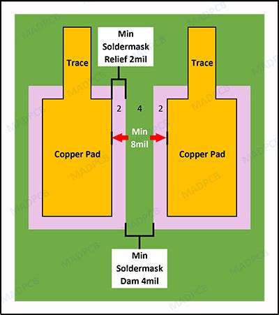
- Solder mask dams or patches to address coverage issues
It is important to document all corrective actions taken and to re-test the PCB after rework to ensure that the soldermask performance meets the required standards.
FAQs
- What is the difference between liquid photoimageable (LPI) and dry film soldermask?
-
LPI soldermask is applied as a liquid and then photoimaged to create the desired pattern, while dry film soldermask is a solid film that is laminated onto the PCB surface and then photoimaged. LPI soldermask is more common due to its higher resolution and finer pitch capabilities.
-
Can soldermask color affect the PCB’s performance?
-
In most cases, soldermask color is chosen for aesthetic or branding purposes and does not directly impact the PCB’s performance. However, some specialized applications may require specific colors for functional reasons, such as white soldermask for LED lighting or black soldermask for high-contrast visual inspection.
-
How does soldermask affect the PCB’s impedance?
-
Soldermask can affect the PCB’s impedance by altering the dielectric constant of the surface layer. This effect is more pronounced at high frequencies and can be addressed by adjusting the PCB design or using a soldermask with a known dielectric constant.
-
What is the typical thickness of PCB soldermask?
-
The typical thickness of PCB soldermask ranges from 0.5 to 2.0 mils (12.7 to 50.8 microns), depending on the application and the soldermask material used. Thicker soldermask layers provide better insulation and protection but may impact the PCB’s dimensions and component placement accuracy.
-
How often should PCB soldermask testing be performed?
- The frequency of PCB soldermask testing depends on factors such as the PCB’s intended application, the production volume, and the quality control requirements. In general, soldermask testing should be performed during the initial PCB prototyping stage, as well as periodically during production to ensure consistent quality. High-reliability applications may require more frequent testing, while lower-volume or less critical applications may have reduced testing frequencies.
Conclusion
Testing PCB soldermask is a critical step in ensuring the quality, reliability, and performance of printed circuit boards. By understanding the various testing methods and their respective advantages and limitations, PCB manufacturers can effectively evaluate soldermask performance and identify potential issues early in the production process.
Regular soldermask testing, combined with thorough interpretation of results and prompt corrective action, helps to minimize the risk of PCB failures and ensures that the final product meets the required industry standards and customer expectations. As PCB technology continues to evolve, staying up-to-date with the latest testing methods and standards will remain essential for maintaining a competitive edge in the electronics manufacturing industry.
Leave a Reply