What Are SMT PCBs and How Do They Benefit Production Time?
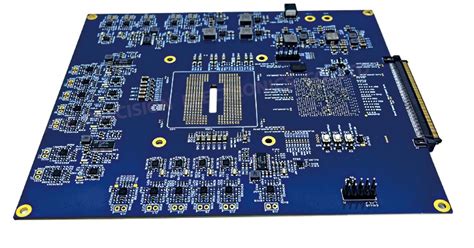
SMT (Surface Mount Technology) PCBs are printed circuit boards where the components are mounted directly onto the surface of the board rather than being inserted into drilled holes. This manufacturing technique has several advantages that can significantly speed up PCB production time compared to through-hole methods.
The key benefits of SMT PCBs for faster production include:
- Automated placement of components
- Smaller component sizes
- Increased component density
- Simultaneous soldering of components
- Fewer drilling steps required
- Streamlined inspection
By leveraging surface mount technology, PCB manufacturers can place components extremely quickly and precisely using automated pick-and-place machines. The smaller size of SMT components also allows for much greater component density, fitting more functionality in less space.
Additionally, all the SMT components can be soldered to the board simultaneously in a single pass through a reflow oven. This is much faster than individually soldering each pin of through-hole components. Fewer holes need to be drilled as well. Visual inspection of proper component placement and soldering is also easier with SMT.
Designing for SMT Manufacturing to Optimize Production Speed
To take full advantage of the production efficiencies of SMT PCBs, the board must be properly designed with surface mount technology in mind from the beginning. Some key design considerations include:
Choosing Appropriate SMT Component Packages
SMT components come in a variety of standardized package types. Smaller chip packages like 0201, 0402, 0603, and 0805 can be placed extremely quickly. However, very small 01005 components may slow down the process. Larger packages like QFP and BGA are placed more slowly but allow for more complex components.
| Package | Imperial Size (in) | Metric Size (mm) |
|---|---|---|
| 01005 | 0.016 x 0.008 | 0.4 x 0.2 |
| 0201 | 0.024 x 0.012 | 0.6 x 0.3 |
| 0402 | 0.04 x 0.02 | 1.0 x 0.5 |
| 0603 | 0.063 x 0.031 | 1.6 x 0.8 |
| 0805 | 0.08 x 0.05 | 2.0 x 1.25 |
| 1206 | 0.126 x 0.063 | 3.2 x 1.6 |
| 1210 | 0.126 x 0.10 | 3.2 x 2.5 |
Choosing mid-size chip packages, SOICs, and SSOPs where possible will provide a good balance of placement speed and component availability. Avoid packages with leads on four sides like QFNs to simplify assembly.
Orienting Components for Efficient Placement
Whenever possible, SMT components should be oriented in the same direction, such as all resistors placed vertically. This allows the pick-and-place machine to populate the board faster. Components should also be aligned to a standard grid with sufficient spacing between parts. A standard grid of 0.5mm is typical.
Panelizing Boards for Parallel Production
Designing multiple copies of the board in a larger array or panel allows many PCBs to be populated and soldered in parallel, greatly increasing throughput. Aim to panelize as many boards as will fit within the machine’s working area, typically about 400x460mm. Provide milling slots, mousebites, or v-score lines to depanelize the individual boards after assembly.

Leveraging SMT Production Techniques for Faster Turnaround
With a PCB designed for SMT, manufacturers can apply additional techniques to further speed up production, such as:
Automated Solder Paste Application
Before placing components, solder paste is applied to the SMT pads. This can be done quickly and precisely by automated paste printers. The paste is applied through a stainless steel stencil with laser-cut apertures that match the pad sizes and locations. Automated optical inspection verifies proper paste volume and alignment in seconds.
Optimized Pick-and-Place Machine Programs
Automated pick-and-place machines can be programmed to optimize their component placement sequence and paths for maximum speed. This involves strategically picking multiple components simultaneously and planning the shortest travel paths between placement locations. Well-optimized programs can achieve placement rates of more than 50,000 components per hour.
Reflow Soldering for Fast and Reliable Joints
After placing components, the entire board is run through a reflow soldering oven which melts the solder paste to form completed solder joints. The oven controls the temperatures precisely to melt the solder without damaging components. Conveyor speeds of 1-2 meters per minute allow boards to be soldered as fast as they exit the pick-and-place machines.

Streamlining Inspection and Test Procedures
Ensuring the PCBs are assembled correctly is critical but can become a bottleneck if not handled efficiently. SMT PCBs enable faster inspection and testing by:
Facilitating Automated Optical Inspection
With components mounted on the surface, automated optical inspection (AOI) systems can quickly check component presence, positioning, and solder joint formation. AOI machines compare high-resolution photos of the assembled PCBs to the expected appearance to detect any issues in seconds.
Enabling Flying Probe Testing
Flying probe testers can quickly test the electrical functionality of the completed SMT PCBs without requiring custom test fixtures. The tester probes can access test points and component pins directly on the surface to verify proper connections and performance. This allows PCBs to be tested in a matter of minutes as soon as they leave the production line.

Case Study: Speeding Up Production of a Consumer Electronics Device
To illustrate the impact SMT PCBs can have on production time, consider a manufacturer producing a handheld consumer electronics device. The original design used through-hole components and took 4 weeks to produce a batch of 5,000 units.
By redesigning the PCB assembly for SMT, the manufacturer was able to achieve the following improvements:
- SMT components placed 5x faster than through-hole insertion
- Panelization allowed 5 PCBs to be assembled in parallel
- Solder paste and reflow soldering eliminated hand soldering bottlenecks
- AOI cut inspection time by 80% compared to manual checks
- Flying probe testing verified functionality in minutes instead of hours
With these SMT optimizations, the total production time for 5,000 units was reduced to less than 1 week – a 4x speedup. The manufacturer was able to bring the product to market a month sooner while also lowering production costs.
FAQ
1. What is the main difference between SMT and Through-hole PCBs?
The main difference is that SMT components are mounted directly onto the surface of the PCB, while through-hole components have leads that are inserted into drilled holes and soldered on the opposite side. SMT allows for smaller components, higher density, and faster automated assembly.
2. Can SMT and through-hole components be used on the same PCB?
Yes, a PCB can be designed with a mix of SMT and through-hole components. This is often done to accommodate through-hole connectors, large power inductors, or other specialized components that may not be available in SMT packages. However, a mix of technologies will not be as fast to assemble as a pure SMT design.
3. What are the limitations of SMT PCBs?
SMT PCBs are not ideal for every application. The small size of SMT components can make manual rework and repair more difficult. SMT assemblies may also be more prone to mechanical stress and vibration damage without additional reinforcement. Very high power applications may require through-hole components for their greater current carrying capacity.
4. How much faster is SMT assembly compared to through-hole?
The speed advantage of SMT varies based on the specific design and components used, but it is typically 3-5 times faster than through-hole assembly. A simple SMT design with chip components may see a 5x speedup, while a complex design with large BGA packages may be closer to a 3x improvement.
5. Are SMT PCBs more expensive than through-hole?
While the SMT components themselves may have a slightly higher cost than equivalent through-hole parts, the total cost of SMT PCB production is usually lower due to the reduced manual labor required. The production speed and efficiency gains typically outweigh any difference in component costs.
Summary
SMT PCBs offer significant advantages for speeding up electronic product development and production. By enabling automated assembly processes and higher component density, SMT can dramatically reduce PCB manufacturing time.
Designing the PCB assembly with the right SMT packages, component orientation, and panelization allows manufacturers to optimize the production process for maximum speed. Techniques like paste printing, pick-and-place programming, and reflow soldering further accelerate the assembly. Automated optical inspection and flying probe testing ensure quality without slowing down the production line.
When properly implemented, SMT PCBs can slash manufacturing times by 70% or more compared to through-hole designs. For bringing products to market quickly and competing in fast-paced industries, SMT is an essential technology for electronics companies to adopt.


Leave a Reply