Understanding Soldermask and Its Purpose
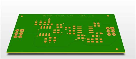
Before delving into the removal process, it’s important to understand what soldermask is and why it is used on PCBs. Soldermask, also known as solder resist or solder stop, is a thin layer of polymer applied to the copper traces of a PCB. Its primary functions include:
-
Protection: Soldermask shields the copper traces from oxidation, corrosion, and physical damage, ensuring the longevity and reliability of the PCB.
-
Insulation: It acts as an insulating layer, preventing accidental short circuits between adjacent traces or components.
-
Solder Control: Soldermask defines the areas where solder should be applied during the assembly process, preventing solder bridges and ensuring precise component placement.
-
Aesthetics: Soldermask gives PCBs their distinctive green color (although other colors are available) and provides a professional and finished appearance.
Reasons for Removing Soldermask
While soldermask plays a crucial role in PCB manufacturing and assembly, there are situations where its removal may be necessary:
-
Repair and Rework: If a PCB has a manufacturing defect or requires modifications, removing the soldermask can provide access to the underlying copper traces for repair or rework.
-
Inspection and Testing: Removing soldermask can facilitate visual inspection of the copper traces, allowing for better examination of potential issues or defects.
-
Prototyping and Experimentation: During the prototyping phase, removing soldermask can enable quick modifications and iterations on the PCB design.
-
Reverse Engineering: In some cases, removing soldermask may be necessary for reverse engineering purposes, allowing for a closer examination of the PCB’s layout and circuitry.
Methods for Removing Soldermask
There are several methods available for removing soldermask from PCBs, each with its own advantages and considerations. Let’s explore some of the most common techniques:
1. Chemical Removal
One of the most effective methods for removing soldermask is through the use of chemical solvents specifically designed for this purpose. These solvents work by dissolving the soldermask material, leaving the underlying copper traces intact. Some popular chemical solvents for soldermask removal include:
- Dimethylformamide (DMF)
- N-Methyl-2-pyrrolidone (NMP)
- Gamma-Butyrolactone (GBL)
- Dichloromethane (DCM)
To use chemical solvents for soldermask removal, follow these steps:
-
Wear appropriate personal protective equipment (PPE) such as gloves, safety glasses, and a respirator to ensure your safety.
-
Place the PCB in a well-ventilated area or a fume hood to avoid inhaling harmful fumes.
-
Apply the chemical solvent to the desired area using a brush, swab, or spray bottle, ensuring even coverage.
-
Allow the solvent to penetrate and dissolve the soldermask for the recommended time (refer to the manufacturer’s instructions).
-
Use a soft brush or a plastic scraper to gently remove the dissolved soldermask from the PCB surface.
-
Rinse the PCB with isopropyl alcohol (IPA) or deionized water to remove any residual solvent and debris.
-
Dry the PCB thoroughly using compressed air or a lint-free cloth.
Chemical removal is highly effective and can remove soldermask quickly and cleanly. However, it’s essential to handle these solvents with care, as they can be harmful if inhaled or come into contact with skin. Always follow the manufacturer’s guidelines and dispose of the solvents properly.
2. Mechanical Abrasion
Another method for removing soldermask is through mechanical abrasion, which involves physically scraping or sanding away the soldermask layer. This method can be suitable for small areas or for removing soldermask from specific components. Some tools commonly used for mechanical abrasion include:
- Abrasive pads or sandpaper (fine grit)
- Fiberglass scratch brush
- Precision knife or scalpel
- Dremel tool with a grinding or sanding attachment
To remove soldermask using mechanical abrasion:
-
Secure the PCB in a stable position to prevent movement during the abrasion process.
-
Select the appropriate tool based on the size of the area and the level of precision required.
-
Gently scrape or sand away the soldermask, applying even pressure and taking care not to damage the underlying copper traces.
-
Use a magnifying glass or microscope to inspect the progress and ensure complete removal of the soldermask.
-
Clean the PCB with isopropyl alcohol (IPA) to remove any debris or dust generated during the abrasion process.
Mechanical abrasion can be effective for targeted soldermask removal but requires a steady hand and careful technique to avoid damaging the PCB. It may be time-consuming for larger areas and can potentially leave scratches or uneven surfaces on the copper traces.
3. Laser Ablation
Laser ablation is a high-precision method for removing soldermask using a focused laser beam. This technique is often used in industrial settings and offers several advantages, such as:
- Precise control over the removal area
- Minimal risk of damaging the underlying copper traces
- Fast and efficient removal process
- Suitable for intricate patterns and fine features
Laser ablation systems typically use fiber lasers or CO2 lasers with high peak power and short pulse durations. The laser beam vaporizes the soldermask material, leaving the copper traces intact. The process is computer-controlled, allowing for accurate and repeatable results.
However, laser ablation equipment can be expensive and may not be readily accessible for individual users or small-scale projects. It is more commonly used in professional PCB manufacturing and rework facilities.
4. Thermal Removal
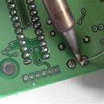
Thermal removal involves heating the soldermask to a high temperature, causing it to soften or burn away. This method can be achieved using a soldering iron, hot air gun, or a dedicated desoldering station. Here’s how to remove soldermask using thermal removal:
-
Set the temperature of the soldering iron or hot air gun to a high setting (around 400°C or 750°F).
-
Gently apply the tip of the soldering iron or the nozzle of the hot air gun to the soldermask, focusing on a small area at a time.
-
Move the heat source slowly and steadily over the soldermask, allowing it to soften and bubble up.
-
Use tweezers or a scraper to carefully remove the softened soldermask from the PCB surface.
-
Repeat the process until the desired area is free of soldermask.
-
Clean the PCB with isopropyl alcohol (IPA) to remove any residue or debris.
Thermal removal can be effective for small areas but requires careful temperature control to avoid overheating and damaging the PCB or nearby components. It may also produce fumes, so adequate ventilation is necessary.

Comparing Soldermask Removal Methods
To help you choose the most suitable method for your specific needs, let’s compare the advantages and disadvantages of each soldermask removal technique:
| Method | Advantages | Disadvantages |
|---|---|---|
| Chemical Removal | – Fast and effective | – Requires handling of hazardous chemicals |
| – Clean and even removal | – Proper ventilation and safety precautions necessary | |
| – Suitable for large areas | – Disposal of chemical waste | |
| ———————- | ———————————————– | ———————————————————- |
| Mechanical Abrasion | – Targeted removal | – Time-consuming for large areas |
| – Minimal setup required | – Risk of damaging copper traces | |
| – Accessible tools | – Uneven removal and potential scratches | |
| ———————- | ———————————————– | ———————————————————- |
| Laser Ablation | – High precision and control | – Expensive equipment |
| – Minimal risk of damaging copper traces | – Limited accessibility for individual users | |
| – Fast and efficient | – Primarily used in industrial settings | |
| ———————- | ———————————————– | ———————————————————- |
| Thermal Removal | – Targeted removal | – Risk of overheating and damaging PCB |
| – Minimal setup required | – Fumes and ventilation concerns | |
| – Accessible tools | – Uneven removal and potential residue |
Safety Considerations
Regardless of the soldermask removal method you choose, it’s crucial to prioritize safety. Here are some important safety considerations to keep in mind:
-
Wear appropriate personal protective equipment (PPE) such as gloves, safety glasses, and a respirator when handling chemicals or working with hot tools.
-
Ensure adequate ventilation when using chemical solvents or performing thermal removal to avoid inhaling harmful fumes.
-
Follow the manufacturer’s instructions and guidelines for handling and disposing of chemical solvents.
-
Exercise caution when using sharp tools or abrasive materials to prevent injury.
-
Work in a clean and organized environment to minimize the risk of accidents or contamination.
Frequently Asked Questions (FAQ)
-
Q: Can I use acetone or nail polish remover to remove soldermask?
A: While acetone and nail polish removers may have some effect on soldermask, they are not recommended for removal. These solvents are not specifically designed for soldermask and may not completely dissolve the material or could potentially damage the PCB. -
Q: Is it possible to selectively remove soldermask from specific areas of a PCB?
A: Yes, targeted soldermask removal is possible using methods such as mechanical abrasion, laser ablation, or thermal removal. These techniques allow for precise control over the removal area, enabling you to expose specific components or traces as needed. -
Q: Can I reapply soldermask after removing it from a PCB?
A: Yes, it is possible to reapply soldermask after removal. However, it requires specialized equipment and materials, such as soldermask ink and a screen printing or spray coating process. Reapplying soldermask may be more challenging for individual users and is more commonly done in professional PCB manufacturing facilities. -
Q: Will removing soldermask affect the functionality of my PCB?
A: Removing soldermask can expose the copper traces to the environment, making them more susceptible to oxidation, corrosion, and physical damage. It is important to consider the purpose of soldermask removal and take necessary precautions to protect the exposed areas. If the PCB will be used in a harsh environment or requires long-term reliability, removing soldermask may not be advisable. -
Q: Are there any alternative methods for soldermask removal besides the ones mentioned in this article?
A: The methods discussed in this article (chemical removal, mechanical abrasion, laser ablation, and thermal removal) are the most common and widely used techniques for soldermask removal. However, there may be other specialized methods or proprietary solutions used in specific industries or applications. It’s always a good idea to consult with PCB manufacturing experts or refer to industry-specific resources for additional guidance.
Conclusion
Removing soldermask from printed circuit boards is a process that requires careful consideration and the right techniques. Whether you choose chemical removal, mechanical abrasion, laser ablation, or thermal removal, it’s essential to prioritize safety, precision, and the integrity of the PCB. Each method has its advantages and disadvantages, and the choice depends on factors such as the size of the area, the level of precision required, and the available resources.
By understanding the purpose of soldermask, the reasons for its removal, and the various methods available, you can make an informed decision and successfully remove soldermask from your PCBs. Remember to follow safety guidelines, work carefully, and consider the long-term implications of soldermask removal on the functionality and reliability of your PCBs.
With the knowledge gained from this article, you are now equipped to tackle soldermask removal projects with confidence and achieve the desired results for your PCB modifications, repairs, or inspections.
Leave a Reply