What is Solder Paste?
Solder paste is a key material used in the assembly of electronic components onto printed circuit boards (PCBs). It is a mixture of tiny solder particles suspended in a flux medium, which helps to clean and protect the metal surfaces during the soldering process. Solder paste is applied to the PCB Pads before the components are placed, and then the entire assembly is heated in a reflow oven to melt the solder and form a permanent electrical and mechanical connection.
Composition of Solder Paste
Solder paste typically consists of the following components:
-
Solder alloy particles: These are tiny spheres of solder alloy, usually made from a combination of tin, lead, and sometimes silver or copper. The most common alloys are Sn63Pb37 (63% tin, 37% lead) and Sn96.5Ag3.0Cu0.5 (96.5% tin, 3% silver, 0.5% copper), also known as SAC305.
-
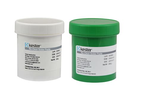
Flux: The flux is a chemical compound that helps to remove oxides and other contaminants from the metal surfaces, promoting better wetting and bonding of the solder. Fluxes can be classified as rosin-based, water-soluble, or no-clean, depending on their composition and how they are removed after soldering.
-
Solvents and additives: These ingredients help to control the viscosity, slump, and other properties of the solder paste, ensuring that it can be easily applied and will stay in place during the reflow process.
Solder Paste Properties
When choosing a solder paste for your assembly process, there are several key properties to consider:
-
Alloy composition: The choice of solder alloy will depend on the specific requirements of your application, such as melting temperature, strength, and compatibility with the components and PCB materials.
-
Particle size: Solder paste is classified by the size of the solder particles, which can range from Type 1 (75-45 microns) to Type 8 (10-5 microns). Smaller particle sizes are generally used for finer-pitch components and more precise deposition.
-
Flux type: The choice of flux will depend on the cleaning requirements and the desired level of residue after soldering. No-clean fluxes are commonly used for most applications, as they leave minimal residue and do not require post-soldering cleaning.
-
Viscosity: The viscosity of the solder paste determines how easily it can be dispensed and how well it will stay in place on the PCB pads. Higher viscosity pastes are generally better for stencil printing, while lower viscosity pastes may be more suitable for dispensing or dipping applications.
-
Slump: Slump refers to the tendency of the solder paste to spread or flow after being deposited on the PCB. A paste with good slump resistance will maintain its shape and position during handling and reflow, ensuring accurate placement of the components.
Storage and Handling of Solder Paste
Proper storage and handling of solder paste are critical to ensuring its quality and performance in the assembly process. Here are some key guidelines to follow:
Storage Conditions
Solder paste should be stored in a cool, dry place, away from direct sunlight and sources of heat or humidity. The recommended storage temperature range is typically between 0°C and 10°C (32°F to 50°F), although this may vary depending on the specific product.
It is important to note that solder paste has a limited shelf life, typically around 6 months from the date of manufacture when stored under proper conditions. The exact shelf life will depend on the formulation of the paste and should be specified by the manufacturer.
Handling Guidelines
When handling solder paste, it is important to follow these best practices:
-
Thawing: If the solder paste has been refrigerated, allow it to thaw completely to room temperature before opening the container. This typically takes around 4-8 hours, depending on the size of the container.
-
Mixing: Before use, the solder paste should be thoroughly mixed to ensure that the solder particles are evenly distributed throughout the flux medium. This can be done using a mechanical mixer or by hand-stirring with a spatula.
-
Avoiding contamination: Solder paste is sensitive to contamination from dust, dirt, and other foreign materials. Always use clean tools and equipment when handling the paste, and avoid touching it with bare hands or exposing it to open air for extended periods.
-
Resealing the container: After use, the solder paste container should be promptly resealed to prevent drying out or contamination. If the paste will not be used again for an extended period, it should be stored back in the refrigerator.
Solder Paste Handling Equipment
There are several types of equipment used for handling and applying solder paste in the assembly process:
-
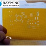
Stencil printers: These machines use a metal stencil to deposit a precise amount of solder paste onto the PCB pads. The stencil is typically made from laser-cut or electroformed metal and has apertures that match the size and shape of the pads.
-
Dispensers: Solder paste can also be applied using automated dispensing equipment, which uses a syringe or valve to deposit a controlled amount of paste onto the PCB. This method is often used for smaller batches or for applying paste to specific areas of the board.
-
Dipping: For some applications, components can be dipped directly into a pool of solder paste before being placed onto the PCB. This method is often used for through-hole components or for rework and repair tasks.
Solder Paste Application Process
The process of applying solder paste to a PCB involves several steps, which may vary depending on the specific equipment and techniques used. Here is a general overview of the process:
Stencil Printing
-
Aligning the stencil: The metal stencil is aligned with the PCB using fiducial marks or other reference points to ensure precise positioning.
-
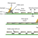
Applying the paste: Solder paste is dispensed onto the stencil and then spread across the surface using a squeegee or metal blade. The paste is forced through the apertures in the stencil and onto the PCB pads.
-
Inspecting the print: After printing, the PCB is inspected to ensure that the paste has been deposited evenly and accurately on all the pads. Any defects or inconsistencies may require cleaning and reprinting.
Component Placement
Once the solder paste has been applied, the components can be placed onto the PCB using automated pick-and-place equipment or manual assembly techniques. The components should be carefully aligned with the pads and pressed down to ensure good contact with the paste.
Reflow Soldering
After the components have been placed, the entire assembly is passed through a reflow oven, which heats the PCB and components to a specific temperature profile. The heat melts the solder particles in the paste, allowing them to flow and form a permanent bond between the components and the PCB pads.
The reflow process typically involves several stages, including:
-
Preheat: The assembly is gradually heated to a temperature just below the melting point of the solder, allowing the components and PCB to equalize in temperature and activating the flux.
-
Soak: The temperature is held steady for a period of time to allow the flux to remove any remaining oxides and prepare the surfaces for bonding.
-
Reflow: The temperature is quickly raised above the melting point of the solder, causing the paste to liquefy and flow around the component leads and pads.
-
Cooling: The assembly is cooled back down to room temperature, allowing the solder to solidify and form a strong, reliable joint.
Inspection and Testing
After the reflow process, the assembLED PCB should be visually inspected for any defects or irregularities, such as bridging, insufficient solder, or misaligned components. Automated optical inspection (AOI) equipment can be used to quickly scan the board and identify potential issues.
Electrical testing, such as in-circuit testing (ICT) or functional testing, may also be performed to verify that the assembly is functioning correctly and meets the required specifications.

Common Solder Paste Defects and How to Prevent Them
Despite careful process control and best practices, several common defects can occur when using solder paste in the assembly process. Here are some of the most common issues and how to prevent them:
Insufficient Solder
Insufficient solder, also known as “dry joints” or “starved joints,” occurs when there is not enough solder paste deposited on the PCB pads to form a complete and reliable joint. This can be caused by several factors, including:
- Stencil apertures that are too small or clogged
- Insufficient Solder Paste Volume or pressure during printing
- Poor paste transfer from the stencil to the PCB
- Excessive slump or spreading of the paste after deposition
To prevent insufficient solder, ensure that the stencil design is optimized for the specific paste and PCB layout, and that the printing process is carefully controlled and monitored. Regular cleaning and maintenance of the stencil and printing equipment can also help to prevent clogging and ensure consistent paste deposition.
Bridging
Bridging occurs when solder paste spreads or slumps across adjacent pads, creating an unintended electrical connection between components. This can be caused by:
- Excessive solder paste volume or pressure during printing
- Poor stencil design or alignment
- Insufficient spacing between pads or components
- Excessive slump or spreading of the paste during reflow
To prevent bridging, ensure that the stencil design provides adequate spacing between pads and that the paste volume is carefully controlled during printing. Using a paste with good slump resistance and optimizing the reflow profile can also help to minimize spreading and bridging during the soldering process.
Solder Balls
Solder balls are small, spherical particles of solder that can form on the surface of the PCB or components during the reflow process. They can be caused by:
- Excessive solder paste volume or pressure during printing
- Poor paste quality or contamination
- Incorrect reflow profile or cooling rate
- Insufficient flux activation or wetting
To prevent solder balls, ensure that the paste volume is carefully controlled and that the reflow profile is optimized for the specific paste and PCB Assembly. Using a high-quality, fresh paste and maintaining a clean, contamination-free environment can also help to minimize the risk of solder ball formation.
Tombstoning
Tombstoning, also known as “drawbridging,” occurs when a small, lightweight component (such as a chip resistor or capacitor) stands up on one end during the reflow process, creating an open circuit or poor connection. This can be caused by:
- Uneven heating or cooling of the component during reflow
- Imbalanced solder paste volume or wetting on the component pads
- Incorrect component placement or alignment
- Insufficient tack strength of the paste to hold the component in place
To prevent tombstoning, ensure that the reflow profile provides even heating and cooling across the entire PCB assembly and that the component placement and paste deposition are balanced and symmetrical. Using a paste with good tack strength and optimizing the placement process can also help to keep components in place during reflow.
Frequently Asked Questions
1. What is the shelf life of solder paste, and how should it be stored?
The shelf life of solder paste is typically around 6 months from the date of manufacture when stored under proper conditions. The paste should be stored in a cool, dry place, away from direct sunlight and sources of heat or humidity. The recommended storage temperature range is usually between 0°C and 10°C (32°F to 50°F), but this may vary depending on the specific product. Always refer to the manufacturer’s guidelines for the exact storage requirements and shelf life of the paste.
2. How do I choose the right solder paste for my application?
When selecting a solder paste, consider the following factors:
- Alloy composition: Choose an alloy that is compatible with your components and PCB materials and meets the requirements for melting temperature, strength, and reliability.
- Particle size: Smaller particle sizes (e.g., Type 4 or higher) are generally better for fine-pitch components and precise deposition, while larger sizes may be suitable for larger components or less demanding applications.
- Flux type: No-clean fluxes are the most common choice for most applications, as they leave minimal residue and do not require post-soldering cleaning. However, other flux types (such as water-soluble or rosin-based) may be necessary for specific requirements.
- Viscosity and slump: The paste should have a viscosity and slump resistance that is appropriate for your deposition method (e.g., stencil printing, dispensing, or dipping) and ensures good print quality and component holding power.
Consult with your solder paste supplier or manufacturer for guidance on selecting the best paste for your specific application and process requirements.
3. How do I optimize the solder paste printing process?
To optimize the solder paste printing process, consider the following tips:
- Use a high-quality, laser-cut, or electroformed stencil with apertures that are optimized for your specific paste and PCB layout.
- Ensure that the stencil is properly aligned with the PCB using fiducial marks or other reference points.
- Control the paste volume and pressure during printing to ensure consistent and accurate deposition on the pads.
- Maintain a clean, contamination-free environment and regularly clean and inspect the stencil and printing equipment.
- Monitor the print quality and inspect the PCB for defects or inconsistencies after printing, making adjustments as necessary.
4. What are some common causes of solder paste defects, and how can I prevent them?
Common solder paste defects include:
- Insufficient solder: Caused by clogged or undersized stencil apertures, insufficient paste volume or pressure, or poor paste transfer. Prevent by optimizing stencil design and printing process.
- Bridging: Caused by excessive paste volume, poor stencil design, or insufficient pad spacing. Prevent by controlling paste volume and ensuring adequate spacing in stencil and PCB layout.
- Solder balls: Caused by excessive paste volume, poor paste quality, or incorrect reflow profile. Prevent by controlling paste volume, using fresh, high-quality paste, and optimizing reflow profile.
- Tombstoning: Caused by uneven heating, imbalanced solder volume, or incorrect component placement. Prevent by ensuring even heating during reflow, balanced paste deposition, and accurate component placement.
Regular process monitoring, quality control, and adherence to best practices can help to minimize the occurrence of these and other solder paste defects.
5. How do I properly dispose of unused or expired solder paste?
Solder paste contains heavy metals and chemical compounds that can be harmful to the environment and human health if not disposed of properly. When disposing of unused or expired solder paste, follow these guidelines:
- Consult with your local environmental regulatory agency for specific disposal requirements and guidelines in your area.
- Do not pour solder paste down the drain or dispose of it in the regular trash.
- Collect the unused paste in a sealed, labeled container and store it safely until it can be disposed of properly.
- Contact a certified hazardous waste disposal company or your solder paste supplier for guidance on proper disposal methods and services.
Always prioritize safe and responsible disposal practices to protect the environment and comply with applicable regulations.
In conclusion, selecting, storing, and using solder paste correctly is essential for achieving high-quality, reliable solder joints in electronic assemblies. By understanding the key properties and requirements of solder paste, implementing best practices for storage and handling, and optimizing the application and reflow processes, manufacturers can minimize defects, improve efficiency, and ensure the long-term performance of their products. Regular training, process monitoring, and quality control are also critical for maintaining consistent results and adapting to new challenges in the ever-evolving world of electronics assembly.

Leave a Reply