What is UV Soldermask?
UV soldermask, also known as solder resist, is a polymer coating applied to the copper traces of a printed circuit board (PCB). It serves several important functions:
- Prevents solder bridges from forming between adjacent pads or traces
- Protects the copper from oxidation and corrosion
- Insulates the circuits, preventing short circuits
- Improves the durability and appearance of the PCB
UV soldermask is applied as a liquid and then cured (hardened) by exposure to ultraviolet light. The unexposed areas are then chemically removed, leaving behind a protective coating in the desired pattern. The most common colors are green, blue, red and yellow, but other colors are available for specialized applications.
Advantages of UV Soldermask Over Other Types
There are a few different types of soldermask used in PCB fabrication. The main advantages of UV curable soldermask include:
| Type | Advantage |
|---|---|
| UV Soldermask | Very fast curing time (seconds vs hours) |
| Excellent resolution of fine details | |
| Superior electrical insulation properties | |
| Harder and more durable surface finish | |
| Better chemical and heat resistance |
Epoxy liquid soldermask and dry film soldermask are more commonly used in large-scale commercial PCB fabs. But for the home PCB maker, UV soldermask offers the best combination of ease of use, performance, and affordable equipment costs.

Materials & Equipment Needed
Before getting started, make sure you have all the necessary supplies on hand:
- Bare PCB board (clean, with no soldermask)
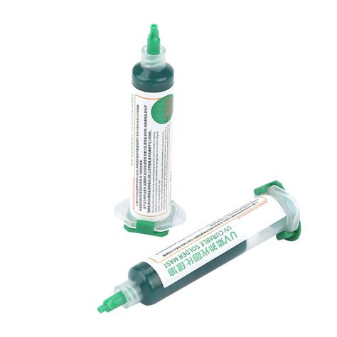
- UV soldermask (available in bottles or pens)
- UV exposure unit with appropriate wavelength output
- Developing tank and rack
- Soldermask developer chemical
- 99% isopropyl alcohol (IPA) for cleaning
- Latex/nitrile gloves, safety glasses, dust mask
- Foam brushes or squeegees for applying soldermask
- Acetate film and laser printer for making exposure masks
- Compressed air for drying
Choosing a UV Soldermask
There are numerous brands and formulations of UV soldermask on the market. For home use, look for ones that are:
- Non-toxic and safe for the environment
- Formulated to be easily applied by hand (proper viscosity)
- Fast curing under UV-A light (320-390nm range)
- Available in small quantities at reasonable prices
Some popular options include:
| Brand | Features |
|---|---|
| Dynamask 5000 | Dip or spray application, fast tack-free cure |
| Epoxies UV22 Soldermask | Brush/dip/spray, UV-A cure, medium viscosity |
| MG Chemicals 419D-P | Pen dispenser, 4oz, various colors, 30 sec cure |
| Solder Mask UV9400 | Screen printable paste, UV cure, lead-free |
Experiment with a few to see which works best for your needs and technique. The subsequent steps will be similar regardless of the exact product used.

Step-by-Step Process
1. Design & Create Soldermask Exposure Masks
The first step is to create a “negative” image mask of where you want the soldermask to remain after developing. You’ll need one mask for each side of the board that has components.
Most PCB design software packages have an option to generate soldermask layers (Gerber file format GTS/GTO). Follow the software instructions to create soldermask layers sized to your specific PCB dimensions.
Print the negative soldermask images onto clear acetate film using a laser printer or photoplotter. You may need to use multiple layers of film to achieve a sufficiently dark mask.
2. Clean & Prepare the Bare PCB
Start with a clean, bare PCB with no soldermask applied. Avoid touching the copper directly with your fingers to prevent oxidation.
Handle the board by the edges and clean both sides with 99% isopropyl alcohol. Use compressed air to fully dry the board. Inspect to make sure there are no defects or contamination on the copper.
3. Apply Liquid UV Soldermask
Put on protective gloves before dispensing and working with the UV soldermask. Refer to the specific product instructions, but the general process is:
- Pour out a line of soldermask onto the PCB surface
- Use a squeegee or foam brush to draw the soldermask across the entire board
- Thoroughly coat all areas of exposed copper with an even layer
- Inspect for full coverage and brush out any bubbles or gaps
- Allow the soldermask to self-level and settle for the recommended time
Repeat the process to coat the other side of the PCB if needed. Work in a low-light environment to prevent prematurely curing the mask before exposure.
4. Expose Soldermask to UV Light
Carefully place the printed acetate mask onto the PCB, aligning it to the edges of the board. For double-sided boards, sandwich the PCB between the two masks, with the ink sides facing the board. Secure with tape if needed.
Place the PCB into a UV exposure unit with the appropriate wavelength for curing your soldermask (usually 365nm). The required exposure time will vary based on:
- The power output of the UV lamps
- The specific soldermask formulation
- Thickness of applied soldermask layer
Refer to the soldermask product recommendations, but exposure times are generally in the range of 30 seconds to a few minutes. Experiment with exposure on test boards to dial in the optimal time.
After exposure, remove the film masks and examine the soldermask. The exposed areas should appear dry and non-tacky. If still wet, give additional exposure time in increments until cured.
5. Develop the Soldermask
Submerge the exposed PCB into a tray filled with soldermask developing solution. Gently agitate the board for the recommended developing time (usually 1-3 minutes). You should see the unexposed soldermask begin to dissolve and rinse away.
After developing, remove the board and immediately rinse it with fresh water. Inspect the PCB to make sure all the unexposed mask has been cleanly removed from the pads and areas that should remain uncoated. Develop longer if needed.
6. Clean and Cure the Soldermask
Thoroughly rinse both sides of the developed PCB with 99% IPA. Use compressed air to dry. Inspect to verify all the soldermask has been removed from pads, holes, and other uncoated areas.
If satisfied, place the board back into the UV unit for a final post-cure exposure. A couple minutes of additional UV light helps to fully cross-link and harden the soldermask for maximum durability.
Allow the PCB to cool down before handling. Inspect the final result under bright light and magnification. Touch up any defects or pinholes with a UV soldermask pen. Your PCB is now ready for final assembly!

Tips for Success
Some parting advice for getting the best possible results when applying UV soldermask at home:
- Practice the entire process on scrap boards first to refine your technique
- Read and follow the pot life, exposure, and curing instructions for your specific soldermask product
- Work in a clean environment to avoid dust or debris contaminating the soldermask
- Experiment with different application methods (dip, spray, brush) to see what works best for you
- Aim to apply a uniform, even coat of soldermask – avoid excess thick or thin areas
- Print exposure masks on high-quality acetate film for optimal density and detail resolution
- Use fresh developer solution and don’t over-develop the boards
- Allow adequate drying and cooling time between process steps
- Consider using a professional vacuum UV exposure unit if doing high volumes of boards
With practice and attention to detail, it’s possible to apply UV soldermask at home that rivals the quality of commercial PCB fabrication houses. It’s a great skill to add to your electronics making repertoire.
FAQ
What’s the shelf life of UV soldermask?
Most UV soldermask products have a shelf life of 6-12 months when stored properly in sealed, opaque containers. Refrigeration can help extend the working life. Always check the expiration date before using and do a test cure on scrap material if in doubt.
Is UV soldermask safe to use?
UV curable polymers are generally safe when used as directed, but it’s important to work in a well-ventilated area and wear proper protective equipment. Gloves, safety glasses, and a vapor mask are recommended. Avoid skin contact or breathing fumes. Refer to the product MSDS for full safety information.
Can I use a regular UV lamp instead of a commercial exposure unit?
For best results, use a high-power UV lamp that emits in the 365nm range and has an even distribution of light. A single UV bulb may be sufficient for small boards, but larger panels will benefit from a multi-lamp exposure unit with a vacuum film holder. A professional unit is a worthwhile investment if you plan to make many PCBs.
How can I remove cured UV soldermask?
Removing soldermask after final curing is difficult and time-consuming. It requires harsh chemicals like concentrated sulfuric acid or methylene chloride. In most cases, it’s easier to scrap the board and start over. To avoid this, be diligent in checking and developing the soldermask before post-curing.
What if I don’t have PCB design software that generates soldermask layers?
If your CAD software doesn’t have automatic soldermask generation, you’ll need to manually create the artwork. Draw solid polygons covering all areas where you don’t want soldermask (pads, holes, etc). Fill in all other areas with solid black. Print these 1:1 scale images mirrored onto acetate film to use as exposure masks.


Leave a Reply