What is Solder Mask?
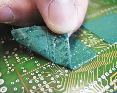
Solder mask, also known as solder resist or solder stop, is a protective coating applied to the copper traces of a printed circuit board (PCB) to prevent accidental short circuits and to protect the copper from oxidation. It is a thin, permanent layer of polymer that is applied to the PCB surface, leaving only the desired exposed copper areas, such as pads and holes, for soldering components.
Solder mask serves several important functions:
- Insulation: It provides electrical insulation between adjacent copper traces, preventing short circuits.
- Protection: It protects the copper from oxidation, scratches, and other environmental factors that could damage the circuitry.
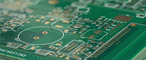
- Aesthetic appeal: Solder mask is available in various colors, with green being the most common, which enhances the visual appearance of the PCB.
Solder Mask Application Methods

There are several methods for applying solder mask to a PCB, each with its own advantages and disadvantages. The choice of method depends on factors such as the desired finish quality, production volume, and cost. The most common solder mask application methods are:
- Screen printing
- Liquid photo imageable (LPI) solder mask
- Dry film solder mask
Screen Printing
Screen printing is a traditional method for applying solder mask to PCBs. It involves the use of a fine mesh screen with a stencil of the desired solder mask pattern. The process follows these steps:
- Solder mask ink is placed on the screen and spread evenly using a squeegee.
- The screen is then placed on top of the PCB, and the squeegee is used to force the ink through the open areas of the stencil onto the board.
- The PCB is then cured in an oven to harden the solder mask.
Advantages of screen printing:
– Cost-effective for low to medium production volumes
– Suitable for simple PCB designs with larger features
– Faster setup times compared to other methods
Disadvantages of screen printing:
– Lower resolution compared to other methods
– Difficulty in achieving consistent thickness across the board
– Limited ability to produce fine details and small openings
Liquid Photo Imageable (LPI) Solder Mask
LPI solder mask is a photopolymer material that is applied to the PCB surface in liquid form and then exposed to UV light to cure and harden. The process involves the following steps:
- The PCB is cleaned and prepared for solder mask application.
- A thin layer of liquid photopolymer is applied to the board surface using a curtain coating or spraying method.
- The coated board is then pre-baked to partially cure the solder mask.
- A photographic film with the desired solder mask pattern is placed on top of the pre-baked solder mask.
- The board is exposed to UV light, which cures the exposed areas of the solder mask.
- The unexposed areas are then removed using a developer solution, leaving the desired solder mask pattern on the board.
- The board is then post-baked to fully cure the solder mask.
Advantages of LPI solder mask:
– High resolution and fine detail capability
– Excellent adhesion to the PCB surface
– Uniform thickness across the board
– Suitable for high-volume production
Disadvantages of LPI solder mask:
– Higher cost compared to screen printing
– Longer processing times due to multiple baking and exposure steps
– Requires specialized equipment and facilities
Dry Film Solder Mask
Dry film solder mask is a solid photopolymer film that is laminated onto the PCB surface and then exposed to UV light to create the desired solder mask pattern. The process involves the following steps:
- The PCB is cleaned and prepared for solder mask application.
- A sheet of dry film solder mask is laminated onto the board surface using heat and pressure.
- A photographic film with the desired solder mask pattern is placed on top of the laminated solder mask.
- The board is exposed to UV light, which cures the exposed areas of the solder mask.
- The unexposed areas are then removed using a developer solution, leaving the desired solder mask pattern on the board.
- The board is then post-baked to fully cure the solder mask.
Advantages of dry film solder mask:
– High resolution and fine detail capability
– Excellent adhesion to the PCB surface
– Uniform thickness across the board
– Suitable for high-volume production
– Faster processing times compared to LPI solder mask
Disadvantages of dry film solder mask:
– Higher cost compared to screen printing
– Requires specialized lamination equipment
– Limited flexibility in adjusting the solder mask thickness
Solder Mask Color Options
Solder mask is available in a variety of colors, with green being the most common. Other popular color options include:
- Blue
- Red
- Yellow
- Black
- White
- Purple
The choice of solder mask color is often based on aesthetic preferences, but it can also serve functional purposes. For example, white solder mask is often used for PCBs with LED components, as it helps to reflect light and enhance the brightness of the LEDs.
Some PCB manufacturers also offer custom color matching services, allowing designers to specify a particular color to match their branding or product aesthetics.
Solder Mask Finish Options
In addition to color options, there are also different finish options available for solder mask. These finishes can affect the surface texture, gloss level, and performance of the solder mask. Common solder mask finish options include:
-
Glossy: A smooth, shiny surface finish that provides a high-quality appearance. Glossy finishes are often used for consumer electronics and other applications where aesthetics are important.
-
Matte: A non-reflective, textured surface finish that reduces glare and provides a more subdued appearance. Matte finishes are often used for industrial and military applications where readability and durability are prioritized.
-
Semi-gloss: A compromise between glossy and matte finishes, offering a moderate level of shine and texture. Semi-gloss finishes are suitable for a wide range of applications.
The choice of solder mask finish depends on the specific requirements of the PCB, such as the intended use environment, aesthetic preferences, and any relevant industry standards or specifications.
Solder Mask Design Considerations
When designing a PCB with solder mask, there are several important considerations to keep in mind:
-
Minimum solder mask clearance: The solder mask clearance is the distance between the edge of a pad or trace and the edge of the solder mask opening. It is important to maintain a minimum clearance to ensure proper insulation and to prevent solder bridging. The minimum clearance depends on the PCB fabrication capabilities and the solder mask application method.
-
Solder mask expansion: During the curing process, solder mask may expand slightly, which can reduce the size of openings and pads. It is important to account for this expansion when designing the PCB layout and specifying the solder mask clearances.
-
Solder mask registration: Solder mask registration refers to the alignment of the solder mask layer with the underlying copper features. Poor registration can result in misaligned openings and exposed copper, which can lead to soldering issues and reduced reliability. It is important to work with a reputable PCB manufacturer that can maintain tight registration tolerances.
-
Solder mask thickness: The thickness of the solder mask layer can affect its insulation properties and durability. A thicker solder mask layer provides better insulation and protection but may also increase the cost and processing time. It is important to specify the appropriate solder mask thickness based on the PCB requirements and the intended use environment.
-
Solder mask compatibility: When selecting a solder mask material, it is important to ensure compatibility with the PCB substrate material, the solderable finish (such as HASL or ENIG), and any other coatings or treatments that may be applied to the board. Incompatible materials can lead to adhesion issues, delamination, or other defects.
By carefully considering these design factors and working closely with a qualified PCB manufacturer, designers can ensure that their PCBs have a reliable and effective solder mask layer that meets the required performance and aesthetic standards.
Frequently Asked Questions (FAQ)
-
What is the purpose of solder mask on a PCB?
Solder mask serves as an insulating and protective layer on a PCB, preventing short circuits between adjacent copper traces and protecting the copper from oxidation and damage. -
What is the most common color for solder mask?
Green is the most common color for solder mask, but other colors such as blue, red, yellow, black, white, and purple are also available. -
What are the main methods for applying solder mask to a PCB?
The main methods for applying solder mask are screen printing, liquid photo imageable (LPI) solder mask, and dry film solder mask. -
What factors should be considered when designing a PCB with solder mask?
Important considerations include minimum solder mask clearance, solder mask expansion, solder mask registration, solder mask thickness, and solder mask compatibility with other materials and finishes. -
Can solder mask be customized to match specific colors or branding requirements?
Yes, some PCB manufacturers offer custom color matching services, allowing designers to specify a particular color to match their branding or product aesthetics.
| Solder Mask Application Method | Advantages | Disadvantages |
|---|---|---|
| Screen Printing | – Cost-effective for low to medium production volumes | – Lower resolution compared to other methods |
| – Suitable for simple PCB designs with larger features | – Difficulty in achieving consistent thickness across the board | |
| – Faster setup times compared to other methods | – Limited ability to produce fine details and small openings | |
| Liquid Photo Imageable (LPI) | – High resolution and fine detail capability | – Higher cost compared to screen printing |
| – Excellent adhesion to the PCB surface | – Longer processing times due to multiple baking and exposure steps | |
| – Uniform thickness across the board | – Requires specialized equipment and facilities | |
| – Suitable for high-volume production | ||
| Dry Film Solder Mask | – High resolution and fine detail capability | – Higher cost compared to screen printing |
| – Excellent adhesion to the PCB surface | – Requires specialized lamination equipment | |
| – Uniform thickness across the board | – Limited flexibility in adjusting the solder mask thickness | |
| – Suitable for high-volume production | ||
| – Faster processing times compared to LPI solder mask |
In conclusion, solder mask is a critical component of PCB manufacturing that provides insulation, protection, and aesthetic appeal to the finished board. The choice of solder mask application method, color, and finish depends on various factors such as the desired quality, production volume, and cost. By carefully considering the design requirements and working with a reputable PCB manufacturer, designers can ensure that their PCBs have a reliable and effective solder mask layer that meets the necessary performance and aesthetic standards. As PCB technology continues to advance, it is likely that new solder mask materials and application methods will emerge, offering even greater flexibility and performance for PCB designers and manufacturers alike.


Leave a Reply