What is LPI Solder Mask?
Liquid photoimageable (LPI) solder mask is a photosensitive polymer coating that is selectively applied to the copper traces of a printed circuit board (PCB). The main purpose of LPI solder mask is to protect the copper traces from oxidation, prevent solder bridges from forming between adjacent pads during the soldering process, and provide electrical insulation.
LPI solder mask offers several advantages over traditional screen-printed solder masks:
- Higher resolution and accuracy
- Thinner and more uniform coating
- Improved adhesion to the copper surface
- Better electrical insulation properties
- Faster and more cost-effective application process
The LPI Solder Mask Application Process
The LPI solder mask application process involves several steps to ensure a high-quality, durable coating on the PCB surface. The main steps in the process are:
- Surface Preparation
- LPI Solder Mask Application
- Pre-baking
- Exposure
- Developing
- Final Curing
Step 1: Surface Preparation
Before applying the LPI solder mask, the PCB surface must be thoroughly cleaned and prepared to ensure proper adhesion of the coating. The surface preparation process typically includes the following steps:
-
Cleaning: The PCB is cleaned using a mild alkaline solution to remove any dirt, grease, or other contaminants from the surface.
-
Micro-etching: A micro-etching solution, usually containing persulfates or peroxides, is used to roughen the copper surface slightly. This process improves the adhesion of the LPI solder mask to the copper.
-
Pre-baking: The PCB is pre-baked in an oven at a temperature of around 80-90°C for 30-60 minutes to remove any remaining moisture from the surface.
Step 2: LPI Solder Mask Application
The LPI solder mask is applied to the PCB surface using either a screen printing or a curtain coating method.
Screen Printing
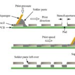
In the screen printing method, a fine mesh screen is used to transfer the LPI solder mask onto the PCB surface. The screen has a negative image of the desired solder mask pattern, with openings allowing the LPI material to pass through onto the PCB.
The screen printing process involves the following steps:
-
The PCB is placed on the screen printing machine, and the screen is positioned above the board.
-
The LPI solder mask is dispensed onto the screen and spread evenly using a squeegee.
-
The squeegee is then used to force the LPI material through the openings in the screen onto the PCB surface.
-
The screen is lifted, leaving a thin, uniform layer of LPI solder mask on the PCB.
Curtain Coating
Curtain coating is an alternative method for applying LPI solder mask, which offers higher throughput and more uniform coating compared to screen printing.
In the curtain coating process:
-
The PCB is passed through a curtain of falling LPI solder mask material.
-
The coating thickness is controlled by adjusting the speed of the conveyor and the flow rate of the LPI material.
-
Excess material is removed using air knives or a similar technique, leaving a thin, uniform layer of LPI solder mask on the PCB surface.
Step 3: Pre-baking
After the LPI solder mask is applied, the PCB is pre-baked in an oven to partially cure the coating and remove any remaining solvents. The pre-baking process is typically carried out at a temperature of around 80-90°C for 15-30 minutes, depending on the specific LPI material being used.
Step 4: Exposure
The pre-baked PCB is then exposed to ultraviolet (UV) light through a photomask, which contains a positive image of the desired solder mask pattern. The UV light causes the exposed areas of the LPI solder mask to polymerize and harden, while the unexposed areas remain soluble.
The exposure process involves the following steps:
-
The photomask is aligned with the PCB, ensuring that the solder mask pattern is correctly positioned.
-
The PCB and photomask are placed in a UV exposure unit.
-
The PCB is exposed to UV light for a specific duration, depending on the LPI material and the thickness of the coating. Typical exposure times range from 30 seconds to several minutes.
Step 5: Developing
After exposure, the PCB is developed to remove the unexposed areas of the LPI solder mask. The developing process is carried out using a mild alkaline solution, which dissolves the non-polymerized regions of the coating.
The developing process involves the following steps:
-
The exposed PCB is immersed in the developing solution for a specific duration, typically ranging from 30 seconds to several minutes.
-
The PCB is then rinsed with water to remove any remaining developer and unexposed LPI material.
-
The developed PCB is inspected to ensure that the solder mask pattern is correctly formed and that there are no defects or residues.
Step 6: Final Curing
The final step in the LPI solder mask application process is to fully cure the coating to achieve its optimal mechanical, chemical, and electrical properties. The curing process is carried out in an oven at a temperature of around 150-160°C for 60-90 minutes, depending on the specific LPI material being used.
During the final curing stage, the polymerization of the LPI solder mask is completed, resulting in a hard, durable, and chemically resistant coating that protects the copper traces and provides electrical insulation.
Advantages of LPI Solder Mask Application
LPI solder mask application offers several advantages over traditional screen-printed solder masks:
-
Higher resolution and accuracy: LPI solder masks can achieve finer feature sizes and more precise alignment, enabling the production of high-density PCBs with smaller pitch components.
-
Thinner and more uniform coating: The LPI Application process results in a thinner and more uniform solder mask layer, which improves the overall flatness of the PCB and facilitates better component placement and soldering.
-
Improved adhesion: The micro-etching step in the surface preparation process enhances the adhesion of the LPI solder mask to the copper surface, reducing the risk of delamination or peeling.
-
Better electrical insulation: LPI solder masks provide excellent electrical insulation properties, minimizing the risk of short circuits and improving the overall reliability of the PCB.
-
Faster and more cost-effective: The LPI application process is generally faster and more automated compared to traditional screen printing, resulting in higher throughput and lower production costs.

Challenges and Considerations in LPI Solder Mask Application
While LPI solder mask application offers numerous benefits, there are also some challenges and considerations to keep in mind:
-
Material selection: Choosing the right LPI solder mask material is crucial to ensure compatibility with the PCB substrate, the desired color, and the required performance characteristics.
-
Process control: Careful control of the application, exposure, and developing parameters is essential to achieve a high-quality, defect-free solder mask layer.
-
Equipment maintenance: Regular maintenance and calibration of the LPI application, exposure, and developing equipment are necessary to ensure consistent results and minimize downtime.
-
Environmental concerns: Some LPI solder mask materials may contain harmful substances, such as volatile organic compounds (VOCs) or heavy metals, which can pose environmental and health risks if not handled properly.
-
Skill requirements: Operators involved in the LPI solder mask application process must be trained and skilled in the various steps, including surface preparation, coating application, exposure, and developing.
FAQ
1. What is the typical thickness of an LPI solder mask layer?
The typical thickness of an LPI solder mask layer ranges from 10 to 50 microns (0.4 to 2 mils), depending on the specific application requirements and the LPI material being used.
2. Can LPI solder masks be applied in different colors?
Yes, LPI solder masks are available in a variety of colors, including green, blue, red, yellow, black, and white. The choice of color depends on the specific application, customer preferences, and any relevant industry standards.
3. How does the LPI solder mask affect the solderability of the PCB?
LPI solder masks are designed to improve the solderability of the PCB by preventing oxidation of the copper pads and providing a flat, uniform surface for component placement and soldering. The solder mask also helps to prevent solder bridges from forming between adjacent pads.
4. What is the shelf life of LPI solder mask materials?
The shelf life of LPI solder mask materials varies depending on the specific formulation and storage conditions. Typically, unopened containers of LPI solder mask can be stored for 6 to 12 months when kept in a cool, dry place away from direct sunlight. Once opened, the material should be used within a shorter timeframe, as specified by the manufacturer.
5. Can LPI solder masks be reworked or repaired?
In some cases, LPI solder masks can be reworked or repaired, depending on the extent and nature of the defect. Small defects or damage may be repaired using specialized solder mask repair kits or by applying additional LPI material and re-exposing the affected area. However, extensive rework or repair may not be feasible, and the PCB may need to be scrapped and replaced.
Conclusion
LPI solder mask application is a critical process in the production of high-quality, reliable PCBs. By selectively applying a thin, photosensitive polymer coating to the copper traces, LPI solder masks offer protection against oxidation, prevent solder bridges, and provide electrical insulation.
The LPI application process involves several steps, including surface preparation, coating application, pre-baking, exposure, developing, and final curing. Careful control of each step is essential to achieve a high-quality, defect-free solder mask layer.
Compared to traditional screen-printed solder masks, LPI solder masks offer several advantages, such as higher resolution and accuracy, thinner and more uniform coatings, improved adhesion, better electrical insulation, and faster, more cost-effective production.
However, there are also challenges and considerations to keep in mind when implementing LPI solder mask application, including material selection, process control, equipment maintenance, environmental concerns, and skill requirements.
By understanding the principles, advantages, and challenges of LPI solder mask application, PCB manufacturers can optimize their processes to produce high-quality, reliable PCBs that meet the ever-increasing demands of modern electronic devices.

Leave a Reply