Printed circuit boards (PCBs) are essential components in nearly all modern electronics. Manufacturing high-quality and reliable PCBs requires careful planning, design, and execution across multiple steps. This article will walk through the end-to-end PCB manufacturing process to understand exactly how these critical boards are made.
PCB Design
The first step in making a new PCB is designing the board itself. This involves using ECAD (electronic computer-aided design) software to map out the board’s circuitry, components, layers, and more.
Key design stages include:
Schematic Capture
This is where the electronic circuit is mapped out showing components like resistors, capacitors, integrated circuits and how they connect. Symbols represent each component.
PCB Layout
The physical PCB layout is created by positioning components and routing the copper traces between them. This layout must match the schematic.
Add Component Footprints
Footprints define the physical size, shape and pin configuration for soldering each component to the PCB.
Route Traces
Traces electrically connect the footprints together as specified in the schematic. Auto-routers can assist but manual tuning is often needed.
Add Power/Ground Planes
Complete power and ground copper layers are added to distribute power across the PCB.
Design Rule Checks
The design is analyzed to catch errors like conflicting footprints or traces. Any violations must be corrected.
Generate Gerber and Drill Files
Final output files are exported, including Gerbers defining each copper layer and NC drill files specifying hole sizes and locations.
Prototype PCB Assembly
Once the design is complete, it’s common to build a small prototype run of PCBs for testing before full production. This validates the design and allows tweaks if issues are found.
Choose Manufacturer
An appropriate PCB manufacturer is selected that meets budget, lead time and quality needs.
Submit Gerber Files
The Gerber files from the design stage are sent to the manufacturer. This provides complete PCB specification.
Select Options
Additional options around PCB materials, finishes, thickness and more are chosen.
Review Manufacturing Plan
The manufacturer reviews the submission and sends manufacturing plan for approval before build.
Manufacturer Builds Prototype
Using the Gerbers and drill files, the PCB maker patterns copper layers, applies finishes, laminates materials, drills holes, etc.
Test Prototype Board
Engineers thoroughly validate board functionality, performance, and durability. Modifications to the design are made if needed.
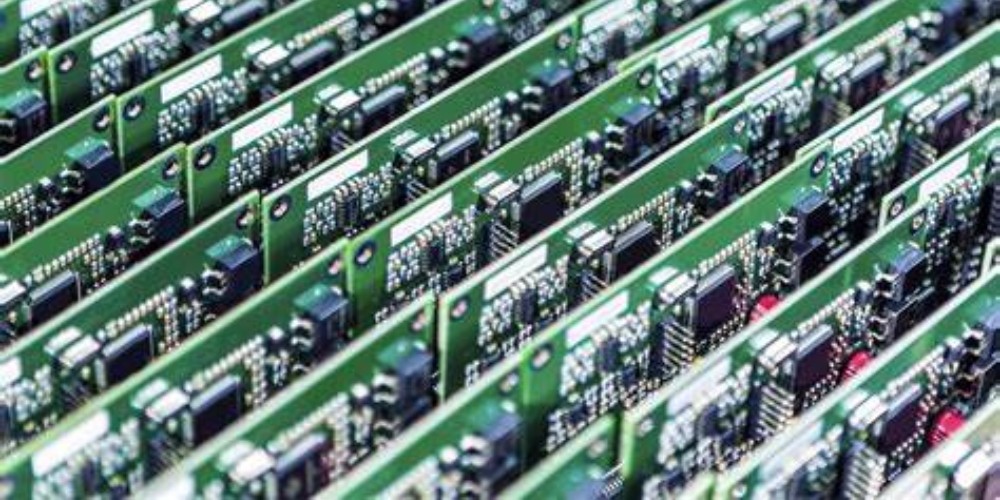
Full Production PCB Manufacturing
Once the design is proven, full production of many boards can begin. The steps are similar but on a much larger scale.
Choose High Volume Manufacturer
For production, an efficient manufacturer with quality processes and cost efficiencies of scale is chosen.
Submit Final Gerber Files
The final release Gerber files are sent to the production manufacturer approved to begin.
Confirm Technical Specifications
All details around layers, materials, finishes, tolerances, testing, etc. are mutually agreed upon.
Place Volume Production Order
A production order is placed for the desired number of boards based on forecasted need and budget. Long lead times often required.
Panelize PCB Layouts
To maximize manufacturing efficiency, multiple PCB layouts are grouped into larger panels that are etched, drilled and routed together.
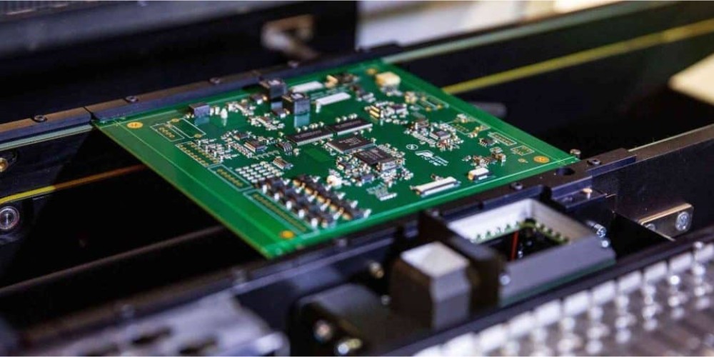
Manufacture through SMT Line
PCBs move through surface mount technology (SMT) lines for automated mass assembly of tiny surface mount components.
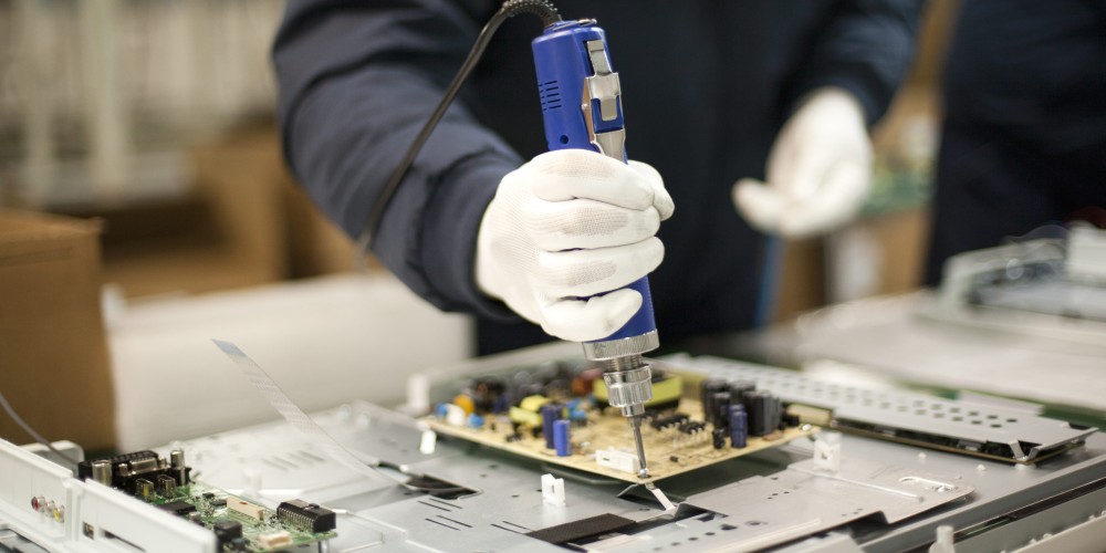
Assemble Other Components
Additional components like connectors, capacitors, heat sinks are manually assembled where automation not possible.
Perform Automated Optical Inspection
Cameras and testing detects errors in assembly or soldering for quality control. Issues are reworked.
Test Functionality
Finished boards are powered on and tested to verify proper functionality before shipment.
Ship to Customer
Once fully manufactured and tested, the PCBs ship out to the customer for integration into their products.
Key PCB Manufacturing Steps
The full end-to-end process involves many sub-steps, but at a high level, these are the core manufacturing stages:
Layer Patterning
The inner and outer copper layers are patterned to form the traces, pads and features. This is done by laminating dry film then exposing and developing it.
Hole Drilling
All through-hole drill locations are precisely drilled at specified sizes through the entire PCB stackup.
Plating and Coatings
Holes are plated with copper and additional coatings like solder, tin or gold are electroplated onto traces.
Lamination
Sheets of dielectric PCB substrate, often FR-4 fiberglass, are stacked and glued together under heat and pressure.
Final Patterning
The outer layers are imaged again to form the traces and features on the outer board surfaces.
Finishing
Edge routing, bevelling, scoring and other processes prepare the boards for shipment and installation.
PCB Manufacturing Techniques
There are a few key techniques used in fabrication PCBs depending on the specific needs:
Subtractive Processes
The copper foil starts out fully covering the substrate. It is etched away subtractively to leave only the desired copper traces behind.
Additive Processes
No initial copper blanket layer is used. Traces are built up additively where needed through electroplating.
Semi-Additive Process
A thin copper layer is laminated. Additional traces are then electroplated on selectively. Provides a compromise approach.
Sequential Lamination
Inner layers are fabricated independently then aligned and laminated together. Allows mixing of layer technologies.
Molded Interconnect Devices (MID)
Laser direct structuring (LDS) can selectively metallize injection molded thermoplastic parts, merging electrical and mechanical functions.
Key Factors in PCB Manufacturing
Several key factors must be optimized during PCB fabrication:
- Registration – Aligning layers and drilling to extremely tight tolerances
- Etch Factor – Producing traces and gaps at the right widths
- Aspect Ratio – Achieving the right plated hole heights and depths
- Via Tenting – Covering holes on outer layers with a thin dielectric layer
- Impedance Control – Managing trace impedances, often for high speed signals
Additional Considerations
For complex or high performance boards, additional steps may be required:
- Soldermask application – Masking areas not to be soldered
- Silkscreen printing – Printing component outlines, labels and identifiers
- Surface finishes – Applying ENIG, immersion tin, or other coatings
- Rework and repair – Fixing flaws found during inspection
- Environmental testing – Heat, vibration, drop and other simulated aging
- Burn-in – Operating boards at high temperature over time to force failures
- Inline inspection – Testing for shorts, opens andchecking for defects during fabrication
- Press-fit insertion – Press-fitting components into plated through holes
- Direct imaging – Laser direct imaging to pattern coatings rapidly
PCB Manufacturing FQA
What are the most important specifications to define when ordering PCB manufacturing?
Some of the most critical specifications to provide are: layer count, board dimensions (x,y), finished copper thickness, minimum trace/space, finished hole sizes, mask over bare copper (MBOC) margin, and netlist for any impedance controlled traces. Providing clear requirements for specifications like these helps ensure the PCB manufacturer can build the boards correctly.
What file formats do PCB manufacturers need for fabrication?
Gerber files (RS-274X) are the standard file format accepted by most PCB manufacturers. This includes separate Gerber files for copper layers, drill files, solder paste layers, soldermask, silkscreen, etc. Many also accept CAD formats like ODB++.
How are very small PCB traces and spaces made during fabrication?
To define ultra-fine lines and spaces below 10 mils, semiconductor-like photolithographic processes are used. Liquid photoresist is deposited on copper layers and then selectively exposed to light through a high-resolution mask. Chemical development then removes either exposed or unexposed areas.
What are volume considerations for PCB production?
For prototypes, as few as 10 PCBs may be ordered. For full production, orders usually start at ~100 boards and often range into the thousands. The largest volumes leverage economies of scale through panelization and automation. Typical minimum orders are around 500-1000 boards.
How long does the PCB fabrication process take?
Lead times for production PCB orders are often 12-16 weeks, sometimes longer. More expedited schedules are possible for additional engineering and setup charges. Building in sufficient lead time is key for new designs to avoid delays during hardware development. Prototypes can be as fast as 24 hours.


Leave a Reply