Understanding Solder Mask and Its Importance
Solder mask, also known as solder resist or solder stop, is a protective layer applied to the copper traces of a printed circuit board (PCB). This layer serves several crucial functions, including:
- Preventing accidental short circuits by isolating the copper traces
- Protecting the copper from oxidation and corrosion
- Providing a more aesthetically pleasing appearance to the PCB
- Improving the durability and longevity of the PCB
Solder mask is typically applied as a liquid photoimageable coating that is then cured using ultraviolet (UV) light. The most common colors for solder mask are green, red, blue, and black, although other colors are available for specialized applications.
Types of Solder mask damage
Despite its protective qualities, solder mask can become damaged due to various factors, such as:
- Mechanical abrasion or scratching
- Exposure to harsh chemicals or solvents
- Improper handling or storage of the PCB
- Manufacturing defects or inconsistencies
When solder mask becomes damaged, it can expose the underlying copper traces, leading to potential short circuits, corrosion, and other issues that can affect the performance and reliability of the PCB.
Assessing the Extent of Solder Mask Damage
Before attempting to repair the solder mask on a PCB, it is essential to assess the extent and nature of the damage. This will help determine the most appropriate repair method and the materials needed.
Visual Inspection
The first step in assessing solder mask damage is to perform a thorough visual inspection of the PCB. Use a magnifying glass or microscope to examine the surface of the board, paying close attention to areas where the solder mask appears to be scratched, chipped, or peeling away from the copper traces.
Continuity Testing
In some cases, solder mask damage may not be readily visible to the naked eye. To detect hidden damage, perform a continuity test using a multimeter. This test will help identify any exposed copper traces that may be causing short circuits or other issues.
To perform a continuity test:
- Set your multimeter to the continuity or resistance mode
- Place one probe on a ground point of the PCB
- Use the other probe to test the continuity between the ground point and various points along the suspected damaged area
- If the multimeter indicates continuity (a low resistance reading or an audible beep), there may be exposed copper in that area

Preparing the PCB for Solder Mask Repair
Once you have assessed the extent of the solder mask damage, you can begin preparing the PCB for repair. This process involves cleaning the damaged area and ensuring that the surface is free of contaminants that could interfere with the repair process.
Cleaning the PCB
- Use a soft-bristled brush or compressed air to remove any loose debris or dust from the surface of the PCB
- Clean the damaged area with isopropyl alcohol (IPA) and a lint-free cloth to remove any grease, oils, or other contaminants
- Allow the PCB to dry completely before proceeding with the repair
Masking Off Sensitive Components
If the damaged solder mask is located near sensitive components, such as microchips or connectors, it may be necessary to mask off these components to protect them during the repair process. Use a high-temperature masking tape or Kapton tape to cover any components that could be damaged by the repair materials.

Repairing Minor Solder Mask Damage
For minor solder mask damage, such as small scratches or chips, there are several methods that can be used to repair the affected area and restore the protective properties of the solder mask.
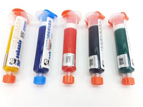
Using a Solder Mask Pen
Solder mask pens are specialized tools that contain a UV-curable solder mask material in a convenient pen-like applicator. These pens allow for precise application of the repair material to the damaged area.
To use a solder mask pen:
- Shake the pen well before use to ensure that the material is evenly mixed
- Carefully apply the solder mask material to the damaged area, taking care not to overlap onto adjacent traces or components
- Use a UV light source (such as a UV flashlight or a specialized UV curing lamp) to cure the material according to the manufacturer’s instructions
- Allow the repaired area to cool and fully cure before handling the PCB further
Applying Liquid Solder Mask
For slightly larger areas of damage, liquid solder mask can be applied using a small brush or applicator. This method allows for more coverage than a solder mask pen but may require more skill and precision to achieve a clean and even repair.
To apply liquid solder mask:
- Dispense a small amount of the liquid solder mask onto a clean, non-porous surface
- Use a fine-tipped brush or applicator to carefully apply the material to the damaged area, avoiding any adjacent traces or components
- Cure the material using a UV light source, following the manufacturer’s recommended exposure times and distances
- Allow the repaired area to cool and fully cure before handling the PCB further

Repairing Extensive Solder Mask Damage
In cases where the solder mask damage is extensive or covers a large area of the PCB, more advanced repair techniques may be necessary. These methods typically involve removing the damaged solder mask and applying a new layer of protective coating.
Removing Damaged Solder Mask
Before applying a new layer of solder mask, the damaged material must be carefully removed from the PCB. This can be done using a combination of mechanical and chemical methods, depending on the extent and nature of the damage.
- Use a fine-grit abrasive pad or sandpaper to gently remove any loose or peeling solder mask material
- For more stubborn areas, a fiberglass scratch brush or a specialized solder mask removal tool may be necessary
- Take care not to damage the underlying copper traces or components during the removal process
- Clean the area thoroughly with isopropyl alcohol (IPA) to remove any debris or contaminants
Applying New Solder Mask
Once the damaged solder mask has been removed, a new layer of protective coating can be applied to the PCB. This process typically involves using a screen printing technique or a specialized solder mask application machine.
For most hobbyists and small-scale PCB manufacturers, outsourcing the solder mask application process to a professional PCB fabrication service is the most practical and cost-effective option. These services have the necessary equipment and expertise to apply a high-quality, durable solder mask layer that will provide long-lasting protection for the PCB.
If you choose to apply the new solder mask layer yourself, follow these general steps:
- Apply a thin, even layer of liquid photoimageable solder mask to the PCB using a screen printing frame or a specialized applicator
- Allow the solder mask to dry according to the manufacturer’s instructions
- Expose the solder mask to UV light using a specialized curing unit, following the recommended exposure times and settings
- Develop the solder mask layer using a suitable developer solution, as specified by the manufacturer
- Cure the solder mask layer using heat and/or additional UV exposure, according to the manufacturer’s guidelines
- Clean the PCB thoroughly and inspect the new solder mask layer for any defects or inconsistencies
Preventing Solder Mask Damage
While it is possible to repair damaged solder mask on a PCB, it is always better to prevent damage from occurring in the first place. By following some simple guidelines and best practices, you can help ensure that your PCBs remain protected and functional for years to come.
Proper Handling and Storage
One of the most common causes of solder mask damage is improper handling and storage of PCBs. To minimize the risk of damage:
- Always handle PCBs by their edges, avoiding contact with the surface of the board whenever possible
- Use clean, lint-free gloves when handling PCBs to prevent the transfer of oils, dirt, and other contaminants
- Store PCBs in a cool, dry place, away from direct sunlight and sources of heat or humidity
- Use anti-static bags or containers to store PCBs, especially those with sensitive components
Choosing High-Quality Solder Mask Materials
When manufacturing PCBs or repairing solder mask, it is essential to use high-quality materials that are specifically designed for the intended application. Cheap or low-quality solder mask materials may not provide adequate protection or durability, leading to premature failure or damage.
When selecting solder mask materials, consider factors such as:
- Compatibility with the PCB substrate material and copper traces
- Resistance to chemicals, solvents, and environmental factors
- Cure time and method (UV, thermal, or air dry)
- Shelf life and storage requirements
- Manufacturer’s reputation and technical support
By investing in high-quality solder mask materials and following the manufacturer’s guidelines for application and curing, you can help ensure that your PCBs are protected by a durable and reliable solder mask layer.
Regular Inspection and Maintenance
To catch solder mask damage early and prevent it from leading to more serious issues, it is important to regularly inspect and maintain your PCBs. This can involve:
- Visually inspecting the PCBs for signs of damage, such as scratches, chips, or peeling solder mask
- Using a multimeter to test for continuity and identify any exposed copper traces
- Cleaning the PCBs regularly with isopropyl alcohol (IPA) and a lint-free cloth to remove dirt, dust, and other contaminants
- Storing PCBs properly and handling them with care to minimize the risk of damage
By establishing a regular inspection and maintenance schedule for your PCBs, you can identify and address solder mask damage early, before it leads to more serious problems or failures.
Conclusion
Solder mask is a critical component of PCB manufacturing, providing essential protection for copper traces and components. When solder mask becomes damaged, it can lead to a range of issues, from cosmetic defects to serious functional problems.
By understanding the importance of solder mask, the types of damage that can occur, and the various methods for repairing and preventing damage, you can help ensure that your PCBs remain protected and functional for years to come. Whether you choose to repair solder mask damage yourself or outsource the task to a professional PCB fabrication service, taking a proactive approach to PCB maintenance and protection is essential for long-term reliability and performance.
FAQs
1. Can I use nail polish to repair solder mask damage?
While some hobbyists have reported using clear nail polish as a temporary fix for minor solder mask damage, it is not recommended as a long-term solution. Nail polish is not designed for use on PCBs and may not provide adequate protection or durability. It is always best to use materials specifically designed for solder mask repair.
2. How long does solder mask take to cure?
The cure time for solder mask depends on the specific material and curing method used. UV-curable solder masks typically require exposure to a UV light source for a specific amount of time, while thermal-cure solder masks may need to be baked in an oven at a specific temperature and duration. Always follow the manufacturer’s guidelines for curing to ensure optimal results.
3. Can I apply new solder mask over existing solder mask?
In most cases, it is not recommended to apply new solder mask directly over existing solder mask. The old solder mask layer may not provide a suitable surface for the new material to adhere to, leading to poor bonding and potential failure. It is best to remove the old solder mask layer before applying a new one.
4. How do I choose the right color of solder mask for my PCB?
The choice of solder mask color is primarily a matter of personal preference or design requirements. Green is the most common color for solder mask, but other colors, such as red, blue, and black, are also widely available. Some specialized applications may require specific colors for functional or aesthetic reasons.
5. Can damaged solder mask cause PCB failures?
Yes, damaged solder mask can lead to a range of PCB failures, including short circuits, corrosion of copper traces, and damage to components. When solder mask is damaged, it exposes the underlying copper traces to the environment, which can lead to oxidation, contamination, and other issues that can affect the performance and reliability of the PCB. Repairing or replacing damaged solder mask is essential for maintaining the long-term integrity and functionality of the PCB.
| Solder Mask Color | Common Applications |
|---|---|
| Green | General-purpose PCBs, consumer electronics |
| Red | High-voltage PCBs, automotive electronics |
| Blue | Medical devices, aerospace electronics |
| Black | High-end audio equipment, luxury consumer electronics |
| White | LED lighting PCBs, reflective surfaces |
| Yellow | Safety-critical applications, warning indicators |


Leave a Reply