Buried vias are an important component in printed circuit boards (PCBs) that allow connections between different layers in the board. Plating of buried vias is a key process that ensures reliable connectivity and allows the vias to serve their purpose. Here is an overview of how buried vias are plated during PCB fabrication.
What are Buried Vias?
Buried vias are vias that connect inner layers of a multilayer PCB without being exposed on the outer surfaces. They are “buried” within the PCB stackup.
Some key points about buried vias:
- They provide interconnections between internal layers only.
- They are not exposed on the top or bottom surfaces of the PCB.
- They are often used to route signals between inner layers.
- They help minimize layer transitions and simplify routing on the outer layers.
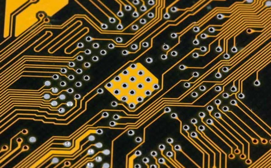
Diagram showing buried vias connecting two inner layers in a 6 layer PCB
Buried vias are fabricated by drilling holes that penetrate the inner layer pairs and then plating the holes to form the electrical connections. The plating process is crucial for buried vias to function properly.
Why Plate Buried Vias?
Plating of buried vias serves several important purposes:
1. Forms Conductive Barrel
Plating deposits conductive metal on the cylindrical wall of the drilled hole to form the via barrel. This creates a continuous conductive path between the layers the via connects.
2. Allows Soldering
Plating allows solder to adhere to the via during component assembly. Solder adhesion is needed for components that connect to buried vias.
3. Prevents Signal Loss
The plating forms a smooth conductive surface that prevents signal loss. Without plating, the rough insulating core material would degrade signal integrity.
4. Improves Reliability
Plating makes the via robust and more resistant to issues like thermal cycling during operation. This improves long term reliability.
5. Facilitates Component Mounting
Plated vias can be used to mount and solder components like BGAs. The smooth solderable surface is important for mounting components.
Proper plating is essential for buried vias to function correctly in the PCB. The plating process takes place after drilling and before lamination.
Plating Process for Buried Vias
Plating of buried vias involves several steps that result in metallization of the via holes. Here is an overview of the plating process:
Step 1 – Drilling
The first step is to drill holes for the buried vias in the inner layer cores using mechanical or laser PCB drilling. High precision is required when drilling to ensure the holes are properly aligned between layers.
The holes penetrate completely through the core layers that will contain the buried vias. But they do not break out to the outer surfaces.
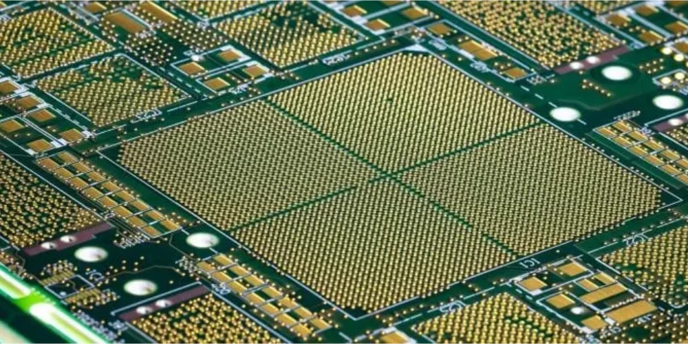
Holes drilled for buried vias in inner layer sections
Step 2 – Desmear
The dielectric core material tends to smear around the edges of the drilled holes. Desmear involves chemically removing this smeared material from the hole walls.
This helps expose the conductive base material of the core layers along the via holes. It also roughens the hole walls to improve adhesion of the subsequent metal plating.
Step 3 – Activation
This step activates the base material of the cores to allow plating adhesion. It usually involves dipping in a palladium catalyst solution. Palladium particles adhere to the hole walls and catalyze the subsequent electroless plating reaction.
Step 4 – Electroless Plating
Electroless copper is plated onto the activated hole walls to provide a thin continuous conductive layer. Electroless plating auto-catalytically deposits copper without any external power source. The palladium acts as the catalyst.
The electroless copper layer is typically 0.5 to 1 microns thick. It covers the hole wall evenly to form the base layer for further plating.
Electroless copper deposits an initial plating layer
Step 5 – Electrolytic Plating
A thicker layer of copper is built up on the electroless layer using electrolytic plating. This involves submerging the PCB stackup in a copper electrolyte bath and applying electric current through the electroless layer.
The electric current causes copper to deposit on the electroless layer. Thicker copper up to 25 microns or more can be plated to form the conductive barrel. The plating thickness depends on the buried via size and required current capacity.
Thicker copper plated with electrolytic process
Step 6 – Strip Plating Resist
Any plating resist used to selectively plate the buried vias is chemically stripped away. This leaves only the plated copper in the vias.
The plated holes are now ready for laminating. The plated barrels form the buried vias after the layers are laminated together.
Key Plating Parameters
Some important process parameters are controlled during buried via plating:
| Parameter | Typical Range | Role |
|---|---|---|
| Hole Wall Roughness | 2-5 μm | Determines adhesion |
| Electroless Thickness | 0.5-1 μm | Base layer for electrolytic plating |
| Electrolytic Thickness | 15-25 μm | Determines current capacity |
| Plating Current Density | 30-90 mA/cm2 | Controls plating rate and quality |
| Plating Bath Temperature | 20-30°C | Affects plating deposition |
The plating parameters are optimized based on the PCB design requirements, buried via dimensions, and fabrication process capabilities.
Plating Equipment Used
Advanced equipment is used to plate high quality buried vias:
- Conveyorized Plating Lines: Automated lines for continuous inline processing of PCB panels. Used for both electroless and electrolytic plating steps.
- Plating Barrels: Rotating barrels used to plate stacked PCB layers. Allow uniform access of chemicals.
- Spray Plating Machines: Use spray nozzles to direct electroless and electrolytic plating solutions at the PCBs for plating.
- Horizontal Plating Tanks: Tank based plating with titanium baskets to hold PCBs in the solutions.
- Pulse Plating Systems: Use pulsed voltage/current waveforms for controlled high quality electrolytic plating.
The specific plating equipment used depends on the PCB fab facility and their production capabilities.
Solder Mask for Buried Vias
After lamination of the plated core layers, solder mask is applied to form the outer board layers. The solder mask coats the entire board surface except areas like pads and vias.
For buried vias, the solder mask layers on the top and bottom surfaces tent over the buried via locations. This prevents the buried vias from being exposed.
The solder mask tenting completely seals the buried vias within the PCB stackup. Only the intended solderable pads are left open through the solder mask.
Solder mask tents cover buried vias on outer layers
This completes the fabrication of high quality plated buried vias as part of the PCB production process.
Advantages of Plated Buried Vias
Compared to alternative solutions like conductive ink filled laser vias, plated buried vias offer several benefits:
- Higher reliability and longer lifetime under thermal cycling stress.
- Ability to withstand high current loads due to thick plated copper barrel.
- Smooth barrel surface prevents signal losses.
- No risk of ink contamination.
- Better soldering and component mounting characteristics.
- Seamless connections to inner layer pads.
- Well established process with proven quality.
Trends in Buried Via Plating
Some emerging trends in plating technology for buried vias:
- Blind Via Plating: Allows plating vias that connect only between adjacent layers rather than all the way through. Provides more flexibility.
- Carbon Nanotube Plating: CNTs are added to the plating chemistry. Creates vias with higher current density and better conductivity.
- Lower Plating Thicknesses: Thinner plated copper barrels help reduce costs and improve high frequency performance.
- Semi-Additive Plating: Uses patterned plating resist rather than subtractive etching to define the plated via. Improves quality.
Frequently Asked Questions
Q: What are the limitations of buried vias?
A: Some limitations include – Limited routing channels due to reduced board space, Unable to probe or repair inner layers, Require advanced drilling precision, Limitations on via current capacity.
Q: Can buried vias be filled or plugged?
A: Yes, buried vias can be filled by plating copper over the hole or using organic plugging material. Via filling improves heat dissipation and reliability. But it adds cost.
Q: Are buried vias only used on multilayer boards?
A: Yes, buried vias require at least 4 conductive layers with dielectric cores in between. They interconnect the inner conductive layers so are only practical on multilayer boards.
Q: How are microvias different from buried vias?
A: Microvias refer to small vias typically under 0.15mm diameter. They can be buried or through-hole vias. Buried specifically refers to vias connecting internal layers without breaching the outer surfaces.
Q: How are buried vias tested for defects?
A: Testing for plating voids or other buried via defects often requires X-ray inspection. Electrical testing can also indicate any faulty connections. Automated optical inspection (AOI) can catch misregistration issues.
This covers the key aspects of how buried vias are plated during PCB fabrication. Proper plating is critical for buried vias to provide reliable interlayer connections in multilayer PCBs. With stringent process controls and advanced plating equipment, high quality plated buried vias can be achieved.


Leave a Reply