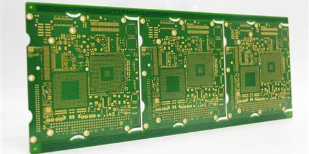
Introduction
High density PCBs, as the name suggests, contain a high number of components and interconnects packed into a small area. With the trend towards miniaturization in electronics, high density PCBs have become commonplace. Designing such complex boards requires careful planning and execution to ensure signal and power integrity while meeting space constraints. This article provides a comprehensive guide to optimizing high density PCB layouts and routing to achieve a robust, high-performance design.
Component Placement
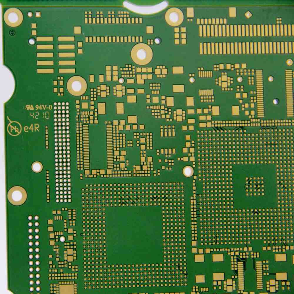
The first step in high density PCB design is strategic component placement. With limited real estate, each part must be positioned optimally to minimize routing congestion. Here are some placement guidelines:
Group Related Circuits
Place components belonging to the same circuit next to each other. This localized grouping minimizes interconnect length and simplifies routing between related parts. For example, place microprocessor near its support components like memories, interfaces, and bus transceivers.
Prioritize Critical Nets
Identify high-speed or noise-sensitive signals and place their drivers and receivers close together. Minimizing trace length on critical nets enhances signal integrity.
Consider Thermal Issues
Ensure adequate spacing between heat-generating components to prevent localized hotspots. Where spacing is limited, use copper fills and thermal vias under the part to conduct heat away.
Allow Space for Routing
Avoid component crowding near board edges or around connectors. Allocate space for trace routing between parts and from parts to connectors.
Follow Assembly Sequence
Place components in the order of assembly. This eases population and rework. Place small SMT devices before larger SMT parts. Through-hole parts are generally placed last.
Creating Effective Power and Ground Networks
With high component densities, delivering clean, stable power is crucial. Some techniques for creating robust power distribution networks (PDNs) are:
Use Multiple Plane Layers
Allocate 2 or more board layers for power and ground to provide low impedance supply networks. 4-layer or 6-layer stacks with complete power/ground plane layers are common.
Provide Adequate Decoupling
Use multiple bypass capacitors for each supply, placed physically close to respective IC pins. 0.1uF and 1uF ceramic caps are typical choices. This suppresses noise and transients on the power rails.
Use Power Islands
Define separate power islands on the PCB for circuit blocks with different voltage requirements. Isolate islands with moats in the power plane. Bridge islands only where necessary using ferrite beads for isolation.
Include Power and Ground Pours
In addition to plane layers, include copper pours for PGND on the top and bottom layers. This provides localized decoupling and heat spreading under parts.
Incorporate PGND Vias
Connect all ground pours and planes using an array of vias. The vias “stitch” ground regions together, minimizing ground bounce and EMI. Use at least 4 vias per stitch.
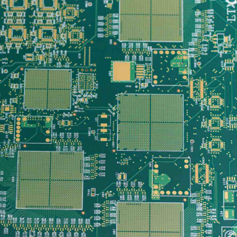
Floorplanning and Blockages
Floorplanning divides the PCB layout into smaller blocks or zones to ease routing. Effective floorplans balance component placement needs with routing requirements. Here are some floorplanning best practices for complex boards:
Define High-Speed Zones
Surround critical traces like DDR, PCIe and high-frequency clocks with ground guard bands to isolate them from noise. Allocate this space upfront.
Allow Space for Test Points
Identify locations needing test points for debug and diagnostics. Reserve space for probe points early, especially on inner layers where accessibility is limited.
Plan for Shielding
If board will be shielded, account for keepouts around shielded sections and allow space for contact fingers along edges.
Leave Routing Channels
Between floorplan blocks, allocate routing channels at least 2-3 times the trace width. Wider spaces may be required near connectors. This eases inter-block routing.
Set Routing Priorities
Plan the order of routing for nets spanning across floorplan blocks. Route critical clocks and high-speed interfaces first. Route lower-priority nets later.
Check Fanout Rules
For BGA parts with pin/ball arrays, ensure the floorplan has space to route traces meeting maximum fanout limits. This avoids necking issues.
Detailed Routing Practices
With placement and floorplanning complete, the focus shifts to routing. Use of appropriate trace topologies, layer usage and termination is key for success.
Select Trace Width and Spacing
Choose widths based on current levels, allowable voltage drop and impedance targets. For spacing, maintain at least 2-3X trace width. Wider spacing required for sensitive analog signals.
Minimize Crosstalk
Avoid running aggressor (noisy) and victim (quiet) traces in parallel over long distances. Use lower layers or cross at 90 degrees to reduce coupling.
Use Layer Transitions Carefully
Route layer changes to avoid discontinuous return paths. Use vias to transition from a trace angle on one layer to match the angle on the next layer.
Terminate Transmission Lines
Use source termination resistors for clock/data outputs. Match trace impedance for optimal termination. Use resistor divider or RC networks for non-matched traces.
Bridge Split Planes
Where a plane like ground is split into islands, bridge the islands on each layer using a grid of stitching vias. This maintains a low impedance ground.
Verify Length Matching
Ensure paired signals have matched trace lengths to avoid skew. Matched propagation delays are critical for differential signals like USB, HDMI, SATA, etc.
Include Test Points
Insert test points on key nets to enable debugging. Test pads on surface layers are ideal. For inner layer traces, use buried or blind vias to bring signals out.
Review Design Rules
Do a final DRC check for errors like width/spacing violations, unconnected pins, etc. Fix violations before manufacturing.
Q&A on High Density PCB Layout
Q: Why is component placement important in high density designs?
A: Strategic placement of parts is crucial because space is limited. Well-planned placement minimizes routing congestion, noise coupling, and thermal issues – resulting in a robust, high-performance design.
Q: What techniques can help reduce crosstalk in dense PCBs?
A: Using lower signal layers, maximizing aggressor-victim spacing, crossing traces orthogonally, surrounding critical nets with ground guards, and using differential signaling helps minimize coupling noise in cramped boards.
Q: How is shielding implemented in high density boards?
A: Shielding cans, metal enclosures and on-board ground planes help isolate sensitive circuitry. Allow space for shields and contacts during floorplanning. Utilize stitching vias to reduce slots in ground planes.
Q: What considerations apply when transmitting high-speed signals in dense PCBs?
A: Match trace impedances, minimize discontinuities, use layer transitions carefully, employ series termination, and equalize trace lengths. This maintains signal integrity at high frequencies when spacing is tight.
Q: Why are multiple power and ground layers recommended?
A: Separate power and ground planes provide low impedance supply distribution in tight spaces. Multiple planes help reduce noise while allowing routing signals on other layers. Proper bypassing and stitching vias enhance PDN performance.
Summary
Designing compact, capable high density PCBs requires careful planning and implementation. An organized component layout, shielding for sensitive circuits, robust power distribution, controlled impedances, minimized crosstalk, and rule-driven routing are essential for success. With an astute floorplan, use of appropriate widths and topologies, controlled terminations, and design rule checks, even the most dense board can be effectively routed. Applying the guidelines discussed here will lead to a high-performing, reliable high density PCB design.


Leave a Reply