Introduction
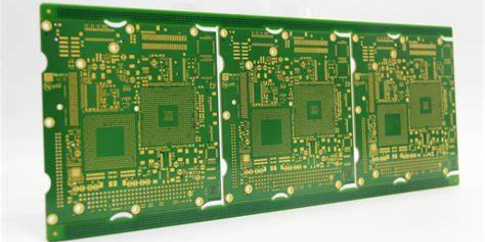
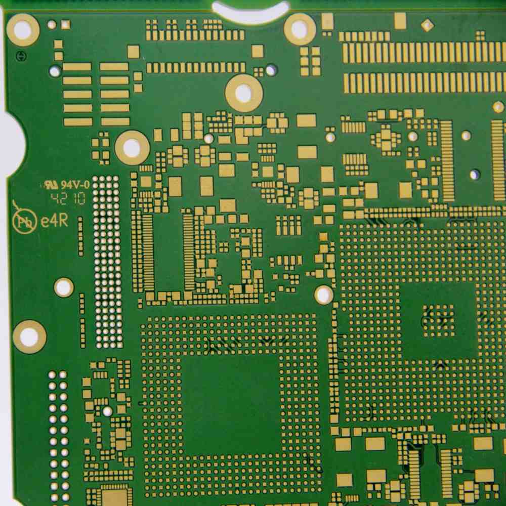
A high density interconnect (HDI) printed circuit board (PCB) is a specialized type of PCB that allows components to be packed more densely on the board. HDI PCBs enable higher routing densities and thinner circuitry than conventional PCBs, making them ideal for advanced, compact electronics designs.
In this comprehensive guide, we will cover everything you need to know about HDI PCBs including:
- What is a high density interconnect PCB?
- Benefits and applications of HDI PCBs
- HDI PCB design and manufacturing considerations
- Comparison to conventional PCBs
- Cost factors for HDI PCBs
- Future trends and innovations
Whether you are new to HDI technology or are looking to utilize it in an upcoming project, this article provides key details on these advanced PCB solutions.
What is a High Density Interconnect PCB?
A high density interconnect or HDI PCB refers to a printed circuit board with a higher component density per unit area than a conventional PCB. This is achieved through three key elements:
1. Fine Line/Space
HDI PCBs utilize thinner copper traces and spaces between traces. While conventional PCB line width/spacing is about 100 microns, HDI boards can have line/space as fine as 25-50 microns. This allows routing of more traces in the same area.
2. Microvias
Microvias are small vias used to interconnect layers on HDI boards. Standard via diameters are around 150-300 microns, but microvias are under 100 microns in diameter (some as small as 25 microns). Using microvias provides vertical interconnects without taking up as much space.
3. Thin Dielectric Layers
HDI PCBs have thinner dielectric insulating layers between copper layers, some as thin as 25-50 microns versus 100+ microns on regular PCBs. This allows packing more circuit layers in a given thickness.
Combining fine line/space, microvias, and thin dielectrics enables greater component densities and multilayer interconnect on HDI boards. Some HDI PCBs have up to 20-50 circuit layers!
| Feature | HDI PCB | Standard PCB |
|---|---|---|
| Line/Space | 25-50 μm | 100 μm |
| Via Diameter | ≤ 100 μm | ≥ 150 μm |
| Dielectric Thickness | 25-50 μm | ≥ 100 μm |
Table: Comparison of HDI PCB and Standard PCB Features
Benefits and Applications of HDI PCBs
HDI PCB technology offers several benefits that make it advantageous for many electronics products:
Smaller and Lighter Products
The main benefit of HDI boards is enabling smaller and lighter end products. Using HDI PCBs allows packing in more components and circuitry within a compact board area. This miniaturization is critical for mobile and handheld devices.
Higher Component Density
Related to the above, HDI PCBs facilitate fitting more components per unit area. This is important for complex, advanced circuit designs. HDI allows high density mounting of ICs like processors, memory, sensors, etc.
More Routing Layers
With thin dielectrics, HDI PCBs can have many circuit layers. This provides routing flexibility to interconnect components across the entire board. HDI is especially useful when routing wide data buses.
Improved Electrical Performance
HDI’s fine features and close spacing mean shorter trace lengths. Shorter trace lengths reduce parasitics for improved high frequency response. HDI PCBs can meet RF/microwave and high speed digital requirements.
Mixed Signal Capabilities
HDI fabrication can integrate both analog and digital circuits on the same board. This facilitates mixed signal devices that combine analog sensors, RF, power circuits with digital processing.
Improved Reliability
Microvias have lower stress and better connectivity than conventional plated through-hole vias. This enhances thermal cycling reliability and via fatigue life. Thin dielectrics also aid reliability.
These advantages make HDI PCB technology well suited for:
- Smartphones, tablets, wearables
- IoT and consumer electronics
- Automotive electronics
- Medical devices
- Aerospace/defense systems
- High speed computing/datacom
- Any application requiring miniaturization, high component density, or electrical performance
HDI provides the highest interconnect density among common PCB technologies.
HDI PCB Design and Manufacturing Considerations
Implementing an HDI PCB requires special design and fabrication considerations:
Advanced PCB Design Rules
HDI PCB layouts require tight design rules and constraints. For instance, trace width/spacing rules, via sizes, and component placement must account for HDI densities. Signal integrity is also important for high speed HDI boards.
Fabrication Tolerances
HDI PCB production demands high accuracy equipment and processes. Lithography, laser drilling, layer alignment, and handling must be done within tight tolerances due to HDI’s fine features. Not all manufacturers can achieve HDI tolerances.
Special Materials
HDI boards require high performance dielectric materials that enable thin cores and fine features. Common materials are high Tg FR-4, polyimides, PTFE composites, ceramic filled hydrocarbon resins. There are fewer material choices than standard PCBs.
Plated Through Hole Limitations
Large plated through holes are problematic for the thin dielectric layers used in HDI boards. Blind/buried vias and microvias are typically used instead of full plated through holes.
Via Fabrication Challenges
Laser drilling small microvias and precisely aligning layers require advanced fabrication expertise. There is a higher risk of defects.
Testing and Inspection Needs
Testing HDI boards for potential fine feature defects using electrical probe testing and other inspection tools require specialized test fixtures and programs.
Cost
Due to tighter design constraints, advanced materials, and precision fabrication, HDI PCBs cost significantly more than conventional PCBs. However, the benefits outweigh the costs for many applications.
Design Expertise
Engineers may need training on HDI design practices. It helps to work with a PCB vendor experienced in HDI early in the design phase.
While demanding, these hurdles are overcome by following sound HDI design principles and choosing a fabrication shop qualified in HDI technology.
Comparison of HDI PCBs to Conventional PCBs
HDI PCBs differ from standard PCB technology in a few key ways:
Component Density
- HDI: High component density with fine features and layers
- Standard PCB: Moderate component density with coarser features
Line/Space
- HDI: 25-50 micron lines/spaces
- Standard PCB: ~100 micron lines/spaces
Number of Routing Layers
- HDI: Up to 20-50 layers
- Standard PCB: Typically ≤ 12 layers
Materials
- HDI: High frequency materials – polyimides, hydrocarbon resins, PTFE composites
- Standard PCB: FR-4 glass epoxy
Viass
- HDI: Blind/buried microvias (<100 micron)
- Standard PCB: Plated through holes (≥ 150 micron)
Fabrication Demands
- HDI: Tight tolerances, advanced processes
- Standard PCB: Relaxed tolerances sufficient
Applications
- HDI: Advanced electronics requiring miniaturization, performance, mixed signal, high density interconnect
- Standard PCB: Cost-effective board solutions without advanced requirements
Cost
- HDI: More expensive
- Standard PCB: Lower cost
In summary, HDI PCB technology enables much higher densities and electrical performance than standard PCBs, but comes at a higher cost and fabrication complexity. It is ideally suited for compact, cutting edge designs.
Cost Factors for HDI PCBs
HDI PCBs generally cost more than conventional PCBs. Here are some of the factors driving HDI PCB pricing:
- Number of layers – More layers equals higher costs. Each layer adds fabrication steps.
- Advanced materials – High frequency laminates used with HDI are more expensive than standard FR-4.
- Tighter tolerances – HDI fabrication must hold tight tolerances, increasing machine and operator costs.
- Microvias – Drilling and plating tiny microvias adds cost versus standard vias.
- Inspection – Fine feature inspection needs advanced testers and programs.
- Limited fabricators – Only high-end fabricators offer HDI capabilities, with proprietary processes.
- Lower yields – Due to HDI’s complexity, yields tend to be lower than standard PCBs, especially on initial designs.
- Smaller market – The HDI market is still a smaller niche compared to conventional PCBs, limiting economies of scale.
- Design complexity – More complex HDI layouts require more engineering work, increasing design costs.
That said, the benefits of HDI often outweigh the higher costs for products requiring small size, light weight, and high performance. And as HDI techniques mature, costs are gradually decreasing.
Future Trends and Innovations in HDI Technology
HDI PCB technology will continue advancing in the future through innovations such as:
- Finer features – Line width/spaces shrinking below 25 microns along with microvias below 50 microns.
- More layers – Continued increases in layer count, with 60+ layer HDI boards becoming feasible.
- Advanced materials – New high frequency laminates to enable higher densities and performance.
- Improved fabrications – Manufacturing enhancements for yield and repeatability of fine geometries.
- Novel interconnects – Integrating fluidic, optical, and other interconnect technologies with HDI.
- Novel applications – Emerging applications like photonics integration, antennas-on-package, advanced RF modules.
- Design tools – Progress with automated design rule checking, modeling, DFM, and custom tool flows tailored for HDI.
- Low cost options – Potential lower cost versions of HDI for cost-sensitive applications.
- Evolution of substrates – Alternatives to traditional laminates, such as thin coreless packages and multilayer buildup boards.
HDI technology will continue pushing the envelope of interconnect density, enabling ongoing electronics miniaturization and performance improvements. Engineers can leverage HDI PCBs to create innovative, advanced products well into the future.
Frequently Asked Questions (FQA)
Here are answers to some common questions about high density interconnect PCBs:
What are the key technologies that enable HDI PCBs?
The three core technologies that allow the high component density of HDI boards are:
- Fine line width and spacing (25-50 microns)
- Microvias with diameters under 100 microns
- Thin dielectric core and buildup layers (25-50 microns thickness)
Combining fine features and thin dielectrics provides the layering and interconnect capability for high density HDI PCBs.
Is HDI PCB technology limited to large companies?
While HDI was once only accessible to large corporations, advances in design tools and contract manufacturing over the past decade have made the technology much more accessible to smaller companies and design teams. With careful design practices and choosing acapable HDI PCB partner, even startups and smaller teams can utilize HDI today.
Can components be placed on both sides of an HDI PCB?
Yes, HDI PCBs typically allow component placement on both the top and bottom sides. The thin dielectrics and microvias of HDI enable connections between components on both sides through the entire board layer stack. This facilitates high density on the surface while also embedding components in the board layers.
Does HDI PCB technology work for both digital and analog/RF designs?
HDI can benefit both digital and analog/RF designs. For digital designs, HDI allows routing complex data buses and power distribution networks across many layers. For RF and analog, HDI’s fine features preserve signal integrity at microwave frequencies. And HDI fabrication can integrate digital and analog circuits on the same board for mixed signal needs.
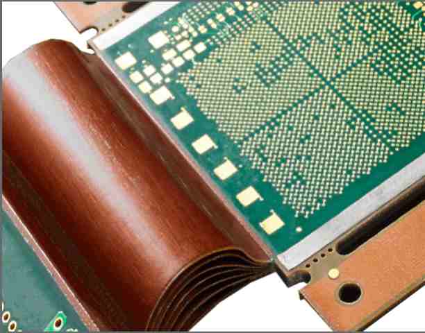
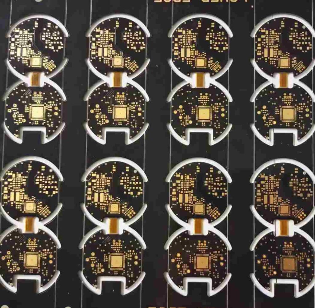
Can flex PCBs be designed with HDI technology?
Yes, HDI can be implemented on flex PCBs as well as rigid boards. Flexible HDI circuits are widely used in foldable mobile devices. The flexible dielectric polymers used in flex PCBs enable HDI trace densities and layer counts. Microvias connect the flex layers together. Careful mechanical design is needed to avoid flexure stresses on microvias.
Conclusion
HDI PCB technology enables revolutionary increases in component packaging densities, interconnect capability, and electrical performance through innovations like fine line width/spacing, microvias, and thin dielectric layers. HDI is ideal for space- and performance-driven electronics across many industries.
While demanding to design and manufacture, the benefits of HDI often make it the optimal PCB technology for cutting edge products. With sound design practices and choosing a capable HDI PCB supplier, engineers can take advantage of this advanced interconnect technology today and into the future.


Leave a Reply