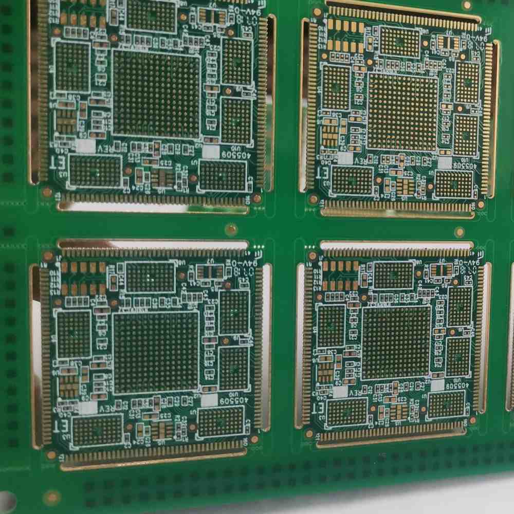
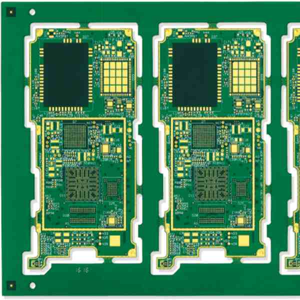
High density interconnect (HDI) PCBs are printed circuit boards with a higher wiring density than traditional PCBs. They allow for denser packing of components and shorter trace lengths, enabling smaller and higher performing electronic devices.
What is HDI PCB?
HDI PCB stands for high-density interconnect printed circuit board. It is a PCB with a higher wiring density than conventional PCBs achieved by using microvias and thin cores.
Key Features of HDI PCBs:
- Fine line spacing and trace widths less than 100 μm
- Microvias with diameters less than 150 μm
- Stacked microvias for even higher wiring density
- Thin dielectric cores (as low as 25 μm)
- More routing layers (up to 20+ layers)
HDI PCBs enable:
- Miniaturization of electronics
- Higher component densities
- Shorter trace lengths for faster signal speed
- Compact form factors
- Advanced functions and capabilities
HDI PCB Construction
HDI PCBs have a specialized layer stackup consisting of stacked microvias and thin dielectric cores:
- Dielectric cores: Thin laminate materials like polyimide used for inner layer insulation. Core thicknesses can be as low as 25 μm.
- Build-up dielectric layers: Thin film dielectrics like ABF or Ajinomoto built up on the surface for traces and vias. Around 40-60 μm thick.
- Microvias: Small vias with diameters less than 150 μm drilled with laser. Used to interconnect buildup layers.
- Stacked microvias: Vias stacked directly over each other in 2-3 levels for high interconnect density.
- Fine lines and spaces: Trace lines and spaces less than 100 μm etched by photolithography.
- High layer count: HDI designs typically have 10 or more routing layers. Advanced designs can have 20+ layers.
This layer stackup with thin cores, microvias, and fine lines/spaces enables the high wiring density of HDI PCBs.
Types of HDI PCBs
There are two main types of HDI PCBs:
1. Sequential Buildup HDI
In sequential buildup HDI, dielectric and trace layers are built up one at a time on top of a solid laminate core:
pros:
- Simpler process
- Lower cost
Cons:
- Only 2-4 buildup layers typical
- Less routing density compared to any-layer HDI
2. Any-Layer HDI
Any-layer HDI alternates laminate cores and buildup layers, enabling a higher number of thinner dielectric layers:
Pros:
- Enables much higher wiring density
- More buildup layers (6+) possible
Cons:
- More complex process
- Higher costs
Any-layer HDI provides the highest interconnect density but at a higher price. Sequential buildup HDI offers a balance of density, cost, and manufacturability.

HDI PCB Design Rules
To achieve the wiring density of HDI PCBs, the design must follow specific guidelines:
Microvia Design Rules
- Microvia diameter: Less than 150 μm, typically 100-125 μm
- Microvia capture pads: At least 120% of drill diameter
- Stacked microvias: Offset at least 50 μm from each other
- Laser drilling provides small diameters with high accuracy
Trace and Space
- Trace width/space: 3/3 mil (75/75 μm) or 4/4 mil (100/100 μm) common
- Thinner traces possible but impact manufacturability
Laminate Cores
- Thin cores improve layer-to-layer capacitance
- Common thicknesses: 35 μm, 60 μm, 100 μm
Stackup
- Total thickness: 200-400 μm allows flexibility while minimizing thickness
- High layer counts help break out complex designs
Following these guidelines ensures HDI PCBs meet the required wiring densities.
HDI PCB Design Software
Specialized PCB design software is required to handle the complex stackups and high pin counts of HDI PCBs. Key capabilities needed:
- Rules-driven stackup planning
- Accurate modeling of HDI stackup
- Microvia and high-density routing tools
- DFM analysis and optimization
- Support for high pin count components
- Manufacturing output generation
Leading HDI PCB design options include:
- Altium Designer – High-speed design and multilayer tools
- Cadence Allegro – Complete PCB solution with HDI features
- Mentor Xpedition – Advanced technologies for cutting edge boards
- Zuken CR-8000 – High-density routing and DFM analysis
The right software allows the intricate layout of HDI designs while ensuring manufacturability.
Applications of HDI PCBs
The benefits of HDI PCBs make them ideal for products where small size, high speed, and advanced functionality are critical:
Consumer Electronics
Smartphones, tablets, wearables, and other compact consumer devices leverage HDI to integrate more features in less space. The high layer counts breakout complex component arrays.
Automotive Electronics
Collision avoidance systems, instrument clusters, engine controllers, and infotainment rely on HDI PCBs. Reliability and quality are necessities in auto applications.
Medical Electronics
Hearing aids, implantable devices, and portable medical electronics achieve miniaturization and signal integrity using HDI PCBs.
Telecom/Datacom
Servers, switches, routers, and base stations in telecom infrastructure employ HDI PCBs for speed, performance, and density. The PCBs connect systems handling immense data flows.
Aerospace/Defense
Avionics, guidance systems, navigation electronics, and communications utilize rugged, reliable HDI PCBs proven for mission-critical applications.
HDI PCBs deliver interconnect performance beyond traditional PCBs, enabling the electronics innovations shaping the future.
HDI PCB Fabrication
Fabricating HDI PCBs requires specialized processes and equipment to handle the tight tolerances and high layer counts.
Key HDI PCB Fabrication Processes:
- Imaging – Fine line lithography patterns buildup layers
- Laser Drilling – Precise laser microvia drilling
- Metallization – Sputtered thin-film metals on buildup layers
- Oxide Treatment – Treat microvias for adhesion
- Copper Plating – Plate up conductors and microvias
- Lamination – Bond core and buildup layers
- Etching – Chemically etch fine features
- Test and Inspection – AOI, flying probe, and more
Advanced equipment needed includes:
- Laser direct imaging (LDI) – For fine line lithography
- YAG lasers – For microvias
- Thin film metallization – For sputtered buildup metals
- Plasma treatment – For microvia adhesion
- High layer count lamination presses – For bonding layers
- AOI and flying probe testers – For verifying quality
The combination of innovative technologies and processes enables reliable, high-yielding HDI PCB fabrication.
HDI PCB Quality Factors
Stringent quality control ensures HDI PCBs meet requirements:
- Dimensional accuracy – Thickness, lines/spaces, hole sizes
- Layer-to-layer registration – For stacked microvias
- Electrical performance – Low resistance, high insulation
Common HDI PCB defects to monitor:
- Over or under-exposed images
- Microvia breakout and capture failures
- Misregistration of layers and microvias
- Conductor defects like opens or shorts
With tight process controls and inspection, HDI PCBs meet the standards for high reliability applications.
HDI PCB Cost Considerations
The specialized fabrication processes result in higher costs for HDI PCBs compared to conventional PCBs. Key factors impacting HDI PCB pricing:
- Layer count – More layers increases costs
- Board thickness – Thinner boards cost more
- Material types – Advanced dielectrics add cost
- Tolerances – Tighter tolerances are more expensive
- Volume – Higher quantities reduce cost
- Lead time – Normal vs. expedited lead times
- Testing – Rigorous testing adds cost
- Certifications – UL, military, aerospace, etc.
In terms of rough order-of-magnitude pricing, HDI PCBs typically range from:
- $500 to $5,000 per design for prototypes
- $200 to $2,000 per board for medium volumes
- $50 to $500 per board for higher production runs
As with any PCB, higher performance and advanced design requirements increase cost. Working closely with your PCB manufacturer is essential to optimizing cost for your HDI design needs.
HDI PCB Challenges and Trends
While delivering major benefits, HDI PCB technology also comes with some challenges:
Signal Integrity
The high component density leads to tight spacing of traces that can cause noise, crosstalk, and impedance issues. Careful stackup planning, routing, and grounding is essential.
Thermal Management
HDI designs concentrate significant power density. Thermal issues like hot spots must be analyzed and mitigated with features like thermal vias.
Manufacturing Yield
The density of HDI PCBs leaves little room for error. Tight process controls are required to maintain yields.
Repair and Rework
Repairing defects in an HDI PCB can be difficult or impossible. Attention to quality is key.
Cost
The specialized fabrication results in higher costs, especially for low volume prototyping.
Current trends in HDI PCB technology aim to address these challenges:
- Advanced thermal management materials and structures
- Higher performance dielectric materials
- Finer lines and spaces below 25 μm
- Improved modeling and analysis software
- Advanced registration and drilling accuracy
- Higher layer counts beyond 20 layers
- Panel-scale manufacturing
HDI PCBs will continue advancing as enabling technologies in leading-edge electronics.
FQA
What is HDI PCB?
HDI PCB stands for high-density interconnect printed circuit board. It’s a PCB fabricated using microvias, thin dielectric cores, and fine lines/spaces to achieve higher wiring density than conventional PCBs.
Why use HDI PCBs?
The high interconnect density of HDI PCBs enables smaller electronics size, higher component density, shorter traces for faster signals, and advanced functionality. Key applications are consumer devices, automotive, aerospace, medical, and telecom.
What are some key features of HDI PCBs?
- Microvias under 150 μm diameter
- Thin cores down to 25 μm
- Fine traces and spaces less than 100 μm
- High layer counts – 10+ routing layers
- Stacked microvias for vertical interconnections
What are the main HDI PCB design rules?
HDI PCB layouts must follow specific guidelines for microvias, trace/space, layer stackup, and more. This includes parameters like 100 μm line/space, 50 μm stacked microvia offset, and core thicknesses under 100 μm.
Why is HDI PCB fabrication more complex?
HDI PCB production requires many specialized processes like laser drilling for microvias, thin film metallization, oxide treatments, lamination of thin cores, and extremely tight tolerances. Advanced inspection is also critical.
How much more expensive are HDI PCBs?
The complex fabrication results in HDI PCBs costing typically 3-5x or more the price of conventional PCBs of similar size. Cost depends heavily on layer count, tolerances, materials, and volume.


Leave a Reply