Introduction
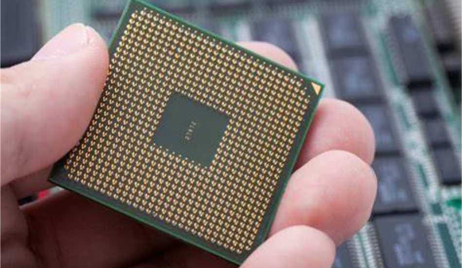
High density interconnect (HDI) is an advanced packaging technology that enables the integration of higher I/O counts, finer lines and spaces, smaller vias, and higher connection pad densities. HDI provides the backbone for next-generation electronics by allowing the interconnection of integrated circuits (ICs) in a smaller, faster, and more efficient format compared to traditional printed circuit board (PCB) technologies. This article provides an in-depth look at HDI technology, its applications, benefits, design considerations, and future outlook.
What is HDI?
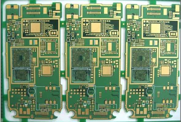
HDI refers to PCBs with a higher wiring density per unit area than conventional PCBs. This is achieved by utilizing thinner dielectric build-up layers and smaller trace/space dimensions to route traces in a high-density gridded 2D architecture.
HDI PCBs utilize stacked microvia structures with trace routing layers on both sides of each sequentially laminated dielectric layer. This allows trace routing between layers and results in shorter, more efficient interconnections. The main benefits of HDI technology include:
- Smaller vias (microvias)
- Finer lines and spaces
- Thinner dielectric build-up layers
- High interconnect trace density
- Improved signal integrity at high frequencies
- Miniaturization of circuit packages
- Increased circuit performance
HDI Microvia Structures
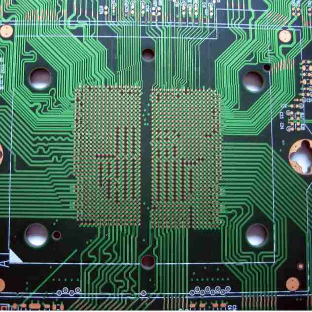
HDI PCBs use stacked microvias to interconnect adjacent thin core dielectric layers. Microvias have diameters smaller than 150 μm (from 50 to 100 μm typically) compared to 300 to 800 μm for conventional plated through-hole (PTH) vias used in standard PCBs.
The most common HDI microvia structures include:
- Stacked microvias: consists of stacked vias connecting multiple built-up layers. The stacked vias are offset from each other and interconnected using short traces.
<p align=”center”> <img src=”https://imgur.com/eiypW0u.png” width=”400″> </p>
- Staggered microvias: similar to stacked microvias but with a more distributed arrangement. Used to optimize routing in dense designs.
<p align=”center”> <img src=”https://imgur.com/tH03MON.png” width=”400″> </p>
- Buried microvias: used to interconnect inner layers of circuitry. Requires precise alignment during lamination.
<p align=”center”> <img src=”https://imgur.com/4HdEIDD.png” width=”400″> </p>
Dielectric Layers
HDI PCBs utilize thinner dielectric layers compared to standard PCBs. Dielectric layer thicknesses of around 50 to 100 μm are typical for HDI, whereas standard PCB dielectric cores are typically 200 to 400 μm thick. Common dielectric materials include polyimide, FR-4, Rogers, and others. Thinner dielectric builds allow fine line routing up to 5/5 μm line/space.
Laser Drilling
Microvias in HDI are typically formed by laser drilling. Laser drilling can produce small diameter vias (50 to 100 μm) with high precision. Other competitive microvia drilling methods include photovia and plasma etching. But laser drilling offers the best capability for high density stacking of microvias on multiple layers.
HDI PCB Technology Generations
The IPC standard IPC-2226 defines four generations of HDI technology with increasing interconnect density:
- 1st generation HDI: Single lamination HDI with stacked microvias connecting two wiring layers per layer pair. Up to 4 mil line/space.
- 2nd generation HDI: Double lamination HDI with stacked microvias connecting two wiring layers per layer pair. Up to 3 mil line/space.
- 3rd generation HDI: Triple+ lamination HDI with stacked microvias connecting two wiring layers per layer pair. Up to 2 mil line/space.
- 4th generation HDI: Same as 3rd generation but with 1 mil line/space capability.
The progression towards higher HDI generations is driven by increasing interconnect density requirements of advanced IC package substrates, wafer level packages, and package-on-package modules.
HDI Benefits and Applications
HDI technology provides several benefits that make it an attractive packaging solution for many advanced electronics:
Miniaturization
- The fine features and dense interconnect capability of HDI allows for significant miniaturization of PCBs and electronic packages. This enables smaller and lighter end products.
High Speeds
- The electrical performance advantages of HDI enable multi-GHz digital signals and high speed communication applications. This includes servers, telecom, defense electronics, etc.
Reliability
- HDI provides excellent thermal cycle reliability performance. The coefficient of thermal expansion (CTE) is optimized by proper matching of dielectric and copper material properties.
Integration
- HDI enables the integration of multiple ICs along with passives and other components in a small footprint package. This is ideal for SiP, SoC, PoP configurations.
Cost
- Despite its advanced capabilities, HDI technology can offer cost benefits compared to ceramics or multi-chip modules for complex package integration requirements.
Some major application areas where HDI PCB technology provides benefits include:
- Smartphones, tablets, laptops
- High speed networking and telecom
- Automotive electronics
- IoT and wearable devices
- Medical diagnostic equipment
- Aerospace and defense systems
HDI is especially useful when there is a need for integrating high I/O density ICs into compact form factors with electrical and thermal performance matching the chip technology.
HDI Design and Fabrication Considerations
Developing a robust HDI PCB or electronic package requires careful design, material selection, fabrication, and testing:
Signal Integrity
At multi-GHz frequencies, maintaining signal integrity on HDI traces is critical. Issues like crosstalk, reflections, attenuation, and EMI need to be analyzed and addressed at the design stage.
Thermal Management
The thermal characteristics like dielectric thermal conductivity, CTE, and Tg need consideration to ensure reliability under thermal cycling. This includes proper dielectric material selection.
DFM Rules
HDI designs require strict design for manufacturing (DFM) guidelines on aspects like microvia capture pads, finish plating, controlled depth drilling, and adequate copper to dielectric ratios.
Stackup Planning
The HDI stackup including dielectrics, copper layers, microvia tiers, and component placement needs optimal planning to meet the electrical, thermal, and reliability objectives.
Fabrication Process Control
The HDI fabrication process – laser drilling, metallization, lamination, etc. – needs to be precisely controlled to produce a high yielding PCB. Automated optical inspection is usually required.
Testing and Inspection
Testing methodologies like ICT, flying probe, and x-ray inspection are mandatory to verify the structural and functional integrity of dense microvia interconnects and thin dielectrics.
With careful design and process considerations, HDI provides a robust and high performance interconnect solution for advanced electronics packaging.
HDI Circuit Architecture Approaches
There are two main HDI circuit architecture approaches used by designers:
Grid Array
This architecture uses a fully gridded routing pattern based on the precision of laser drilled stacked microvias. Microvias act as nodes in the grid network and traces run along the x and y grid lines. Simpler layout but less flexible routing.<p align=”center”> <img src=”https://i.imgur.com/l1BI0GM.png” width=”300″> </p>
Random Routing
This architecture leverages the flexibility of laser drilled microvias to place them anywhere along traces as needed. Provides the most flexible and optimized routing tailored to each design but involves more complex layout considerations.<p align=”center”> <img src=”https://i.imgur.com/SGNkt2c.png” width=”300″> </p>
Grid array architecture is easier to implement but random routing offers most efficient utilization of HDI capabilities for performance driven products.
Future Outlook for HDI Technology
HDI continues to evolve, driven by the roadmaps of semiconductor ICs and advanced packaging techniques like 2.5D/3D integration. Here are some future developments on the horizon for HDI:
- Finer microvias below 50 μm diameter along with <1 μm traces using semi-additive processes (SAP).
- Adoption of new dielectric materials with lower loss tangent and tunable CTE.
- Improved thermal management techniques like thermal vias, buried heat spreaders, etc.
- Embedding of active and passive components into HDI substrate for ultimate miniaturization.
- Leveraging HDI advances made in packaging for next-generation high density PCBs.
- Automating design and fabrication processes for quick turnaround of complex HDI circuits.
- Growth in HDI usage for medical, automotive, and defense applications besides traditional niches.
With its inherent technological and cost scalability, HDI will continue permeating across the electronics packaging landscape in this decade.
Conclusion
In summary, HDI is an interconnect technology that provides the backbone for integrating advanced ICs into miniaturized and high performance electronics packages and PCBs. With its fine features, excellent electrical and thermal performance, design flexibility, fabrication maturity, and cost economies, HDI delivers an optimal solution for next-generation electronics. As ICs continue to evolve, HDI will provide the sophisticated interconnection highway matching the capabilities of silicon chips.
Frequently Asked Questions
Here are some common questions about HDI PCB technology:
Q1. What are the key advantages of using HDI instead of a conventional PCB?
The main advantages of HDI are higher interconnect density, smaller vias and traces enabling miniaturization, improved high speed signal integrity, excellent reliability, and the ability to integrate multiple ICs in a compact package.
Q2. What are some typical applications suiting HDI technology?
Some major application areas that benefit from HDI are smartphones, networking equipment, aerospace electronics, medical equipment, automotive electronics, IoT devices, and other high performance and compact electronics.
Q3. What design factors require special consideration for HDI?
Critical HDI design aspects include maintaining signal integrity at GHz speeds, thermal management, HDI fabrication process design rules, optimal stackup planning, and incorporating sufficient testing.
Q4. How are microvias formed in HDI PCBs?
The microvias used in HDI PCBs to interconnect layers are typically formed by laser drilling. This allows the precise and repeatable creation of small diameter (50-100 micron) microvias.
Q5. What is the future outlook for HDI technology evolution?
HDI continues to evolve with finer features, new materials like low loss/low Dk dielectrics, embedding of actives/passives, thermal management techniques, automated processes, and growth into new application areas besides telecom/Defense.


Leave a Reply