Introduction
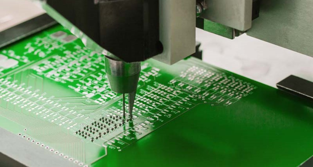
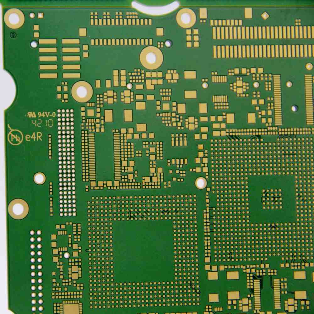
Printed circuit boards (PCBs) form the backbone of most electronic devices we use today. The components on a PCB are connected by copper tracks, called traces, etched onto the board. In order to connect these traces between different layers of the PCB, plated through holes called vias are used. Vias form the interlayer connections that allow signals to travel between layers.
One way to categorize vias is by looking at their Hole Density Index (HDI). HDI refers to the ratio of the via hole diameter to the via pad diameter. Vias can be classified as high density or low density. Understanding HDI vias is important for PCB designers as it impacts factors like manufacturing feasibility, cost, reliability and signal integrity. In this article, we will look at what HDI vias are, their classification, challenges with using them, and some best practices to implement them effectively in your designs.
What are HDI Vias?
Vias with a low HDI ratio, meaning the via pad diameter is much larger than the hole diameter, are considered low density vias. Typically, a via with HDI ratio below 0.3 is considered low density. These vias can have larger hole diameters and are easier to manufacture.
High density interconnect (HDI) vias have a higher HDI ratio, meaning the pad diameter is only slightly larger than the hole diameter. Usually vias with HDI ratio above 0.5 are considered HDI vias. They typically have smaller hole diameters, allowing greater via densities to be achieved. The benefit of higher via densities is that more routing channels are created, allowing for greater routing flexibility.
Here is a comparison of a low density and HDI via:
| Via Type | Hole Diameter | Pad Diameter | HDI Ratio |
|---|---|---|---|
| Low Density | 0.2 mm | 0.6 mm | 0.33 |
| HDI | 0.1 mm | 0.15 mm | 0.67 |
As we can see, the HDI via has a much smaller pad diameter compared to hole diameter, giving it a higher HDI ratio.
HDI Via Classification

HDI vias can be further classified based on the aspect ratios involved:
Class 1 HDI Vias
These vias have an aspect ratio of less than 1:1. This means the thickness of the board is greater than the diameter of the via. These vias are easier to manufacture.
Class 2 HDI Vias
Here the aspect ratio is 1:1 to 4:1, meaning the via diameter is greater than board thickness but less than 4 times the thickness. These pose some manufacturing challenges.
Class 3 HDI Vias
These vias have the highest aspect ratio of greater than 4:1. The diameter is much greater than the board thickness. Manufacturing class 3 HDI vias requires advanced processes and equipment.
Challenges with HDI Vias
Using HDI vias also poses some challenges:
- Manufacturing complexity – Producing boards with HDI vias requires more advanced manufacturing with tighter tolerances. This increases fabrication costs.
- Signal integrity – HDI vias with smaller pad diameters can cause impedance discontinuities which distort signals traveling through them. Careful modeling is required to ensure signal integrity is not compromised.
- Reliability – Plating smaller holes consistently can be difficult, leading to reliability issues due to poor plating. The high aspect ratios of HDI vias also increase thermomechanical stress, impacting reliability.
- Testing – It becomes difficult to probe and inspect boards with HDI vias during manufacturing testing due to the small pad sizes. Specialized testing is required.
HDI Via Design Guidelines
Despite the challenges, the benefits of HDI vias have made them an essential tool for PCB designers. Here are some guidelines to follow when working with them:
- HDI vias should be used judiciously. Reserve them for critical traces that require the additional routing flexibility. Use low density vias when possible.
- Minimize the length of traces passing through HDI vias as longer lengths increase impedance discontinuity effects.
- Model HDI vias in your design software to obtain accurate views of signal integrity performance.
- For higher reliability, use Class 1 or 2 HDI vias. Avoid using Class 3 vias unless absolutely necessary.
- Follow manufacturer design rules and employ any recommended pad styles to ensure plating reliability.
- Discuss HDI via requirements early with your board fabrication vendor. Get their input on manufacturability given your board stackup.
- Use design for manufacturing (DFM) and design for testing (DFT) techniques tailored to HDI vias.
By following these guidelines and working closely with your PCB manufacturer, you can effectively leverage HDI vias and benefit from their increased routing flexibility without compromising quality or reliability.
Example HDI Via Implementation
Here is an example of using an HDI via in a PCB design to route a critical signal path:
In this 8 layer board stackup, we needed to route a high speed clock signal from the microprocessor on Layer 2 to a peripheral on Layer 6. Due to lack of routing channels on the inner layers, this critical track could not be properly routed with low density vias.
Introducing a Class 2 HDI via with 0.1mm hole diameter and 0.15mm pad diameter allowed us to route this track vertically between Layers 2 and 6. The HDI via provided the additional routing flexibility needed while minimizing impact on signal integrity compared to a Class 3 via. Careful modeling was done to optimize the design.
Conclusion
HDI vias enable greater routing densities, providing PCB designers valuable flexibility to connect critical intra-layer paths. However, exercising care when using them is important to manage fabrication complexity, cost, signal performance and reliability. When designed properly, HDI vias become an indispensable tool rather than an obstacle. As PCBs continue getting more complex and compact, skillful application of HDI vias will remain key for unleashing the full routing capabilities of your designs.
FAQ
What are some typical HDI via pad sizes and hole diameters?
For Class 1 and 2 HDI vias, typical pad diameters range from 0.15mm to 0.30mm. Hole diameters are usually between 0.1mm to 0.15mm. Class 3 HDI vias can have even smaller pad/hole sizes down to 0.05mm or less.
Can I split a high speed signal across multiple HDI vias?
It is generally not recommended. Each HDI via will introduce impedance discontinuity which can distort and reflect the signal. Use a single larger HDI via instead or route the critical signal layer adjacently using plane layers.
Do HDI vias reduce the number of routing layers required?
Not necessarily. HDI vias provide routing flexibility but do not reduce actual board layer count in most cases. The smaller vias consume less space, allowing routing channels to be created within the layers. So HDI vias allow better utilization of the available routing layers.
Can I escape fine pitch BGAs with HDI vias?
Yes, the small diameter HDI vias can help escape dense component pads when clearance is extremely tight between pads. This makes them suitable for high density BGA escape routing.
What special considerations are needed for HDI via in pad?
For HDI microvias placed within component pads, ensure the manufacturer can plate the via properly without overplating the pad. This may require coordinate with the vendor on special pad styles to get the right plating balance.


Leave a Reply