Introduction
HDI (High Density Interconnect) technology has revolutionized the printed circuit board (PCB) industry over the past few decades. As electronic devices continue to get smaller and more complex, PCBs must pack more components into less space without sacrificing reliability or performance. HDI provides solutions to fit more interconnects on a PCB while meeting the challenges of finer lines, smaller vias, and closer spacing.
This article will explore the evolution of HDI technology and how it enables higher density interconnects on PCBs. We’ll look at key innovations in HDI processes, materials, and design that allow PCBs to achieve greater functionality in ever-shrinking products.
What is HDI Technology?
HDI refers to technology that allows routing of traces and vias on a PCB with very tight spacing between conductors. The IPC-2226 specification defines HDI PCBs as having:
- Line width/spacing of ≤ 100μm (3.9 mils)
- Via diameters of ≤150μm (5.9 mils)
- Capture pad diameters of ≤300μm (11.8 mils)
By comparison, standard PCB technology typically has:
- Line width/spacing of ≥ 125μm (5 mils)
- Via diameters of ≥ 200μm (8 mils)
- Capture pad diameters of ≥ 400μm (16 mils)
HDI technology uses several innovations to achieve finer feature sizes:
Laser Drilling
Mechanical drilling of vias larger than 150μm often causes smearing, tearing, and damage. Laser drilling achieves consistent, high-precision holes down to 25μm for microvias. Lasers also drill tapered profiles better suited for electroplating vias.
Thin Dielectrics
Standard PCBs use dielectric core layers around 200μm thick. HDI builds up layers of 15-50μm thin laminates, which allow for finer lines and closer via spacing.
Build-Up Layers
HDI PCBs often use semi-additive processes to build interconnect layers directly on the surface rather than laminating clad cores. This allows greater control over trace geometry.
Microvias
Smaller vias act as interlayer connections between trace layers. Stacking these microvias enables vertical system integration by routing signals across several thin HDI layers.
By combining these technologies, HDI provides the high trace density and layer interconnectivity needed for advanced PCBs.
A Brief History of HDI Technology
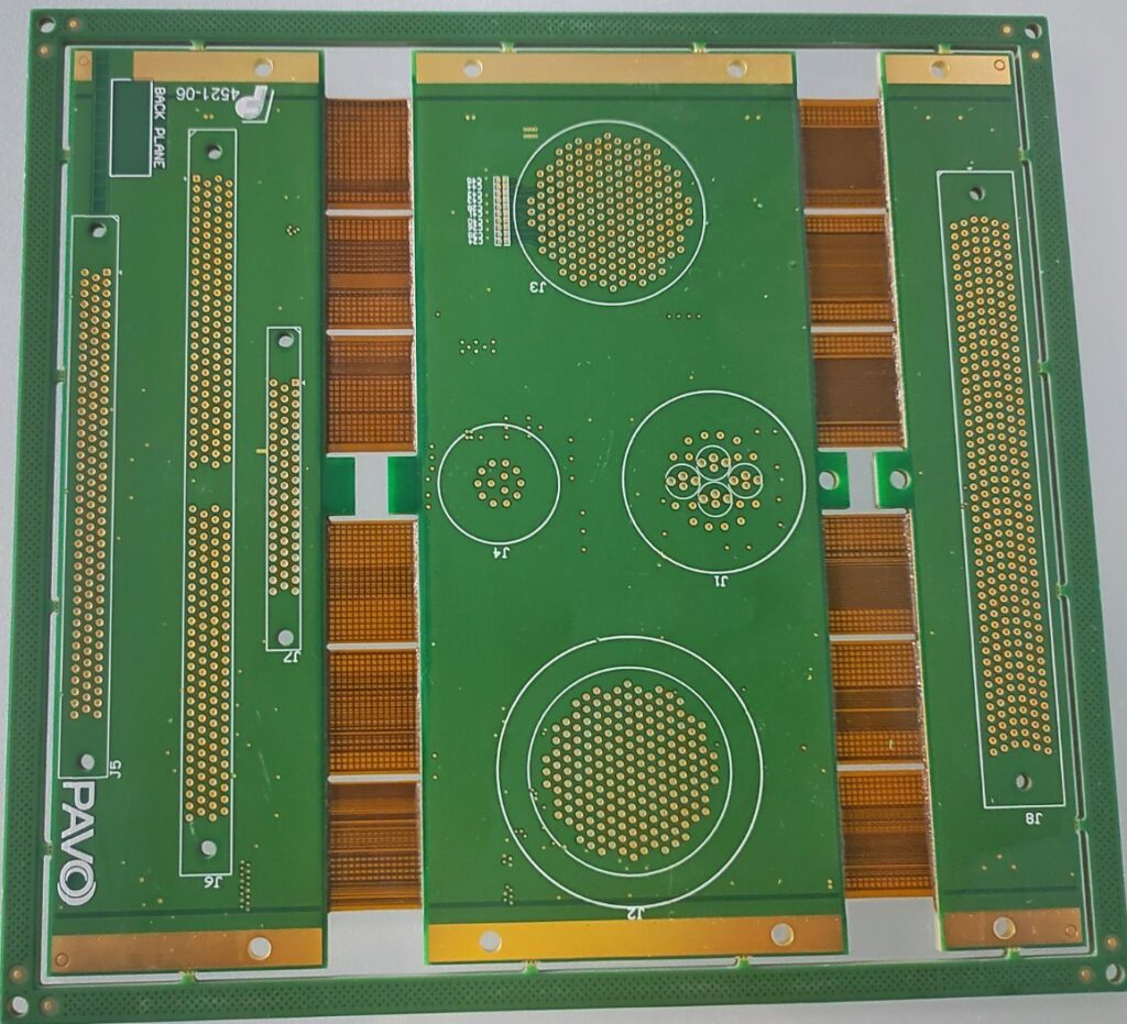
The origins of HDI trace back to the 1980s, when PCB technologists pushed the limits of conventional etching and drilling processes. Multichip modules (MCMs) drove initial demand for HDI with their requirements for dense interconnections between ICs. Here are some key milestones in the development of HDI:
- 1980s – Materials and processes developed to produce multilayer boards with 30-50μm lines and spaces.
- 1994 – Motorola introduces any-layer HDI allowing connections between any conductive layers.
- 1996 – Standards introduced for HDI design, materials, and reliability testing.
- 2000s – Widespread adoption of HDI for mobile product PCBs. Microvia technology matures.
- 2010s – HDI widely used in consumer electronics. Laser drilling enables high-volume HDI production.
- Today – HDI accounts for over 30% of the global PCB market, enabling products like smartphones.
From humble beginnings working with materials like polyimide, the HDI PCB industry has grown enormously based on enabling technologies like laser drilling, finer line lithography, and build-up processes. HDI continues to evolve and improve as demands on PCBs grow.
HDI Layer Stackup and Interconnect Architecture
A key advantage of HDI is the ability to route traces and vias across multiple thin dielectric layers. Here are some examples of HDI layer stackups and interconnect architectures:
2+N+2 Stackup
This simple HDI stackup uses outer microvia layers to route to/from an inner conventional PCB core:<img src=”https://i.imgur.com/6MnUK6P.png” width=”400″>
The core provides most of the mechanical strength while the HDI layers route I/O and high-density local connections. The microvias provide connections between layers.
Any-Layer Stackup
More advanced HDI stackups interleave microvia layers between thin dielectric cores:<img src=”https://i.imgur.com/VnQ4Sf9.png” width=”400″>
This provides the maximum routing flexibility by allowing connections between any two layers. The multiple thin dielectrics also reduce capacitance and crosstalk.
Pad on Microvia
Microvias can connect directly to component pads, rather than routing horizontally to a capture pad:<img src=”https://i.imgur.com/Bg1zFHg.png” width=”300″>
This allows high-density routing very close to component footprints.
The stackup architecture provides extensive flexibility to route complex HDI designs. Innovations like any-layer microvias and pad on microvia provide interconnect efficiency.
HDI Design and Fabrication Considerations
While HDI provides many benefits, it also poses challenges for design and PCB fabrication:
Signal Integrity
Thin dielectrics allow tighter routing, but also increase impedance mismatches, crosstalk, and susceptibility to noise or EMI. Careful route planning, ground planes, and matched length traces help mitigate these issues.
Thermal Management
HDI’s thin, thermally resistive dielectric layers can cause localized heating, especially on power planes. Thermal vias, pads, and planes help conduct heat efficiently.
Registration Accuracy
Aligning layers with tight tolerances is critical for HDI. Advanced laser direct imaging (LDI) pattern generators provide the precision needed.
Via Reliability
With high interconnect density, HDI designs must minimize mechanical and thermal stresses on small vias to ensure reliability. Filling vias improves strength and heat dissipation.
Warpage Control
Closely spaced thin dielectrics require careful lamination processes to minimize warpage. Balanced metal layers help keep HDI PCBs flat.
While designing and making HDI PCBs is complex, the benefits of small, high-performance electronics make the effort worthwhile.
Applications of HDI Technology
The high routing density, thin profiles, and advanced integration capabilities of HDI provide key advantages across many end products:
Consumer Electronics
Smartphones, tablets, and wearables must pack maximum functionality into extremely compact and lightweight packages. HDI allows these devices to integrate processors, memory, sensors, and wireless communications without growing in size.
Automotive Electronics
HDI provides automotive-grade reliability and thermal stability for engine control units, infotainment, radar, and other in-vehicle electronics.
Medical Devices
Implantable and portable medical devices use HDI to achieve complex, multilayer PCBs in small volumes. Biocompatible materials are also available.
Aerospace and Defense
Ruggedized HDI boards meet the reliability demands of avionics and military electronics while minimizing size and weight.
IoT Products
Compact HDI PCBs allow smaller IoT modules and products with greater functionality. HDI will continue growing in usage as IoT devices become smaller.
From handheld gadgets to self-driving cars, HDI enables electronics to deliver amazing capabilities and performance in ever-shrinking packages.
The Future of HDI Technology
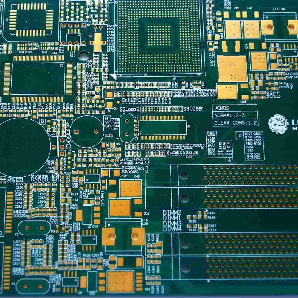
As product requirements continue advancing, HDI innovation marches onward. Here are some emerging HDI technologies to watch:
- Any Layer Microvias Below 20μm – Even finer interconnects coming soon.
- Low-Loss, High-Speed Materials – New dielectrics address signal integrity issues.
- Thermal Management Materials – Enhanced thermally conductive core, prepreg, and filling materials.
- Fine Line Semi-Additive Processes – Tighter tolerances for build-up layers down to 20μm lines and spaces.
- Wafer-Scale Packaging – Thin, large HDI boards embedding or soldering die and components.
- Flexible/Rigid HDI – Bendable circuits with high density on flexible polymer cores.
- Heterogeneous Integration – Mixing HDI, silicon, and other technologies in one package.
HDI began from stretching the limits of PCBs, and that innovative spirit continues today. As electronics advance, we can expect HDI technology to rise to the challenge.
Conclusion
HDI has transformed PCB capabilities over recent decades and become indispensable for products requiring small, high-performance electronics. While HDI fabrication poses difficulties, the benefits of denser interconnects with thinner profiles continue driving its widespread adoption. With the ongoing evolution of materials, processes, and designs, HDI technology will remain critical for enabling the electronics of tomorrow.
Frequently Asked Questions
What are the key benefits of using HDI technology?
The main benefits of HDI technology are:
- Increased routing density from finer lines and closer spacing
- Thinner overall PCB thickness by using thin dielectric layers
- Flexibility to route traces and microvias between any layers
- High interconnectivity from microvias, enabling more signal channels
- Miniaturization of products by packing more circuits into less space
How does HDI compare in cost to standard PCB technology?
In general, HDI PCBs have a 15-35% cost premium over conventional boards. The specialized materials, demanding fabrication processes, lower yields, and precise imaging tools required contribute to the higher costs. However, HDI allows reducing the overall system size and component counts, helping offset the board price premium through savings elsewhere.
What are the main reliability concerns with HDI PCBs?
Some of the key reliability risks using HDI include:
- Microvia cracking from stresses
- Fracturing or delamination of thin dielectric layers
- Overheating due to higher current densities
- Signal loss or interference due to thin dielectrics
- Reduced thermal cycling lifetime compared to thicker boards
Careful design practices, thorough testing, and advanced fabrication processes help mitigate these concerns and produce robust, reliable HDI circuits.
Are there design differences between HDI and standard density PCBs?
Yes, designing for HDI requires some different approaches:
- Stackup planning for layer interconnectivity
- Minimizing trace lengths for thinner conductors
- Managing impedance with precise line width and dielectric control
- Allowing for decreased thermal dissipation through thin cores
- Tight registration and tolerances between layers
- Considering reliability risks and wearout modes
What PCB technology might eventually replace HDI?
Some emerging technologies like embedded trace substrates and molded interconnect devices provide routing density comparable to HDI without using laminated dielectric layers. But HDI has continued evolving alongside new technologies and still provides advantages. The next major shift may come from integrating PCBs directly with ICs or packaging using wafer-scale or panel-level processes.
Leave a Reply