Introduction to HDI Technology
HDI (High Density Interconnect) is a printed circuit board (PCB) manufacturing technology that allows for higher circuit densities and more compact designs compared to traditional PCB fabrication. HDI enables more routing channels and smaller via diameters, allowing for complex circuitry integration in a smaller physical space.
Some key characteristics of HDI technology:
- Allows tracing and spacing of under 6 mil
- Permits microvias with diameters as small as 3-5 mil
- Enables build-up layer circuitry with stacked microvias
- Reduces pad sizes and pitch for finer pitch components
- Increases wiring density with thin core or coreless constructions
HDI circuit boards are ideal for compact, high performing products such as smartphones, tablets, wearables, medical devices, and more. As electronics continue trending towards miniaturization and mobility, HDI provides the advanced fabrication techniques to meet these demands.
Benefits of Using HDI
Some of the major benefits that HDI technology offers include:
- Higher Component Density – The fine lines, traces, spaces, and microvias of HDI allow for more connections per unit area, enabling integration of more components.
- Miniaturization – HDI fabrication techniques facilitate size reduction of PCB assemblies, critical for portable electronics and devices where space constraints exist.
- Signal Integrity – Smaller vias, optimized trace routing, and tightly controlled impedances help maintain signal integrity at high frequencies.
- Layer Count Reduction – By shifting routing to the HDI build-up layers, fewer layers are needed in the board core, reducing costs.
- Improved Reliability – Plated through holes are eliminated in favor of microvias, removing a common failure point.
- Design Flexibility – HDI provides more routing channels, allowing creativity in laying out tight circuit connections.
HDI Structures and Constructions
There are several types of HDI board constructions that offer different advantages:
1. Build-Up HDI
This uses a conventional PCB core (typically FR-4) with additional build-up dielectric and copper layers laminated on top to form the HDI structure. The I/O pads connect through the core layers to the build-up layers.
2. Coreless HDI
As the name implies, coreless HDI boards eliminate the core FR-4 layers and implement the HDI build-up layers directly on a thick copper foundation. This enables the thinnest constructions but are prone to warpage without a core for stability.
3. Any-Layer HDI
Any-layer HDI incorporates microvias in every layer of a multilayer board, rather than just the outer build-up layers. This maximizes connection options between layers but requires advanced drilling precision.
4. Sequential Build HDI
Sequential build HDI involves successive lamination of dielectric and copper foil layers, with each lamination fully imaged and etched before the next is added. This allows greater control and yields the finest features.
5. High-Density Interconnect Flex
HDI technology has also expanded into flex PCB fabrication, combining the flexibility of flex circuits with the integrated capabilities of HDI to offer robust solutions where bending is required.
HDI Design and Layout Considerations
To effectively implement HDI in your PCB design, keep these guidelines in mind:
- Use CAD tools capable of the finer features sizes and clearances required
- Minimize trace lengths for high speed signals for optimal performance
- Watch for impedance matching and crosstalk between traces
- Limit the number of microvia transitions in critical signal paths
- Ensure components are compatible with the reduced pad and pitch dimensions
- Account for increased layer-to-layer registration tolerances
- Provide adequate trace widths for required current
- Plan panel utilization carefully to control warpage and stresses
HDI Microvia Technology
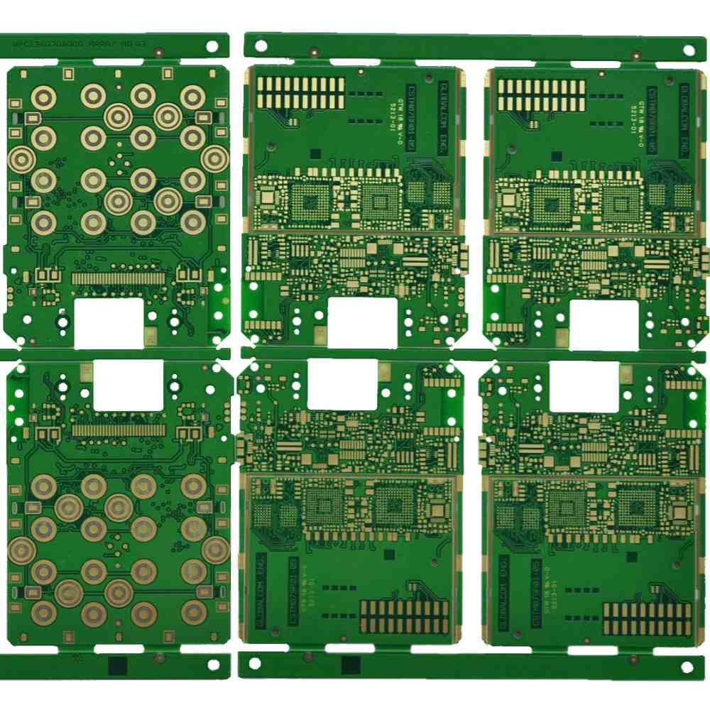
A microvia is a small plated through hole that electrically connects HDI conductive layers in a PCB. The most distinguishing feature of HDI circuit boards is the extensive use of microvias in the design. Standard PCB vias range from 8 to 12 mils in diameter. In contrast, microvia diameters typically fall between 3 to 8 mils.
The reduced size of microvias is a critical technology that facilitates the miniaturization and component density achievable with HDI. By shrinking the vias, finer routing features can be implemented in the layers above and below. Microvias also improve electrical performance by reducing parasitic capacitance and insertion losses at high frequencies compared to traditional vias.
Key Benefits of Microvias
- Enable trace and space of 4 mils or below
- Allow higher wiring densities
- Reduce parasitic inductance and capacitance
- Improve signal integrity at high speeds
- Permit greater routing flexibility
- Decrease layer requirements and cost
Microvia Challenges
While microvias offer significant advantages, their ultra-small dimensions also impose fabrication and reliability challenges including:
- Precise Drilling Accuracy – Laser drilling must be tightly controlled to hit targets as small as 3 mils and avoid creating defects.
- Thin Dielectric Concern – Thin dielectrics between layers increases the risk of microvia barrel cracking during layers lamination.
- Reliable Metallization – Achieving reliable plating of ultra-small via holes requires optimized chemical processing.
- Registration Control – Tighter registration tolerances are necessary to ensure landing pads line up across layers.
- Aspect Ratio Limits – Maintaining low microvia aspect ratios reduces reliability risks from stresses.
Microvia Design Rules
Key microvia design guidelines include:
- Minimum microvia diameter is typically 3 to 5 mils
- Maximum aspect ratio (height/diameter) of 1:1 to 1:3
- Capture pads should allow for +/- 0.5 to 1 mil registration tolerance
- Avoid placing microvias in high current paths
- Limit the daisy chaining of microvias (use stacked vias instead)
- Minimize the number of layer transitions through microvias where possible
Following these rules will help maximize microvia manufacturability and performance.
Stacked Microvia Technology
To increase routing capacity in HDI boards while mitigating microvia reliability risks, stacked microvias are often used. Stacked microvias involve placing two or more microvias immediately adjacent to each other, essentially creating one larger conductive channel. This provides several advantages:
Benefits of Stacked Microvias
- Allows routing high current paths not achievable with individual microvias
- Reduces risk of microvia cracking by lowering aspect ratios
- Spreads stresses across multiple vias versus concentrating in one
- Decreases layer transitions for better signal integrity
- Increases process margin by creating larger capture pads
- Enables higher interconnect densities
Stacking two 3 mil diameter microvias creates an effective 5 mil via, for example, providing more cross-sectional copper area for currents without consuming more routing space on the layers. Stacked microvias do come with some disadvantages, however:
Stacked Microvia Drawbacks
- Potential for increased parasitic capacitance if not routed carefully
- Requires precise laser driller accuracy to align vertically
- Increased cost compared to single microvias
- More difficult to plug if necessary for unused vias
For HDI designs carrying signals with fast edge rates or higher current, stacked microvia configurations are an important tool for enhancing performance and reliability. When routing moderate frequency digital signals, single microvias may be sufficient.
HDI Line Width/Space
In addition to microvia technology, HDI fabrication also supports much finer conductive trace dimensions compared to standard PCB processes. While standard PCB technology achieves trace widths and spaces down to around 6 mils, HDI is capable of 4 mil and even smaller features.
Advantages of Fine Line Widths
- Increase routing channels for higher component density
- Allow placement of finer pitch components
- Improve signal quality with closely matched traces
- Reduce parasitic inductance, capacitance and losses
- Facilitate miniaturization of circuit dimensions
Considerations for Thin Traces
- Ensure adequate current carrying capacity
- Account for increased impedance and coupling
- May require thinner copper or finish plating
- Watch for susceptibility to handling damage
- Maintain minimum web width around drilled holes
Design Guidelines
Some typical HDI line width/space design rules:
- Minimum trace width: 4 to 5 mils
- Minimum space between traces: 4 to 5 mils
- Thinner traces may require thicker copper foil
- Wider traces above ~8 mils for high current paths
- Tightly control impedances for matched length traces
HDI technology empowers PCB designers with an expanded toolbox of options for routing complex circuits. But with the benefits of smaller features come additional considerations for manufacturability, performance, and reliability.
HDI Board Materials
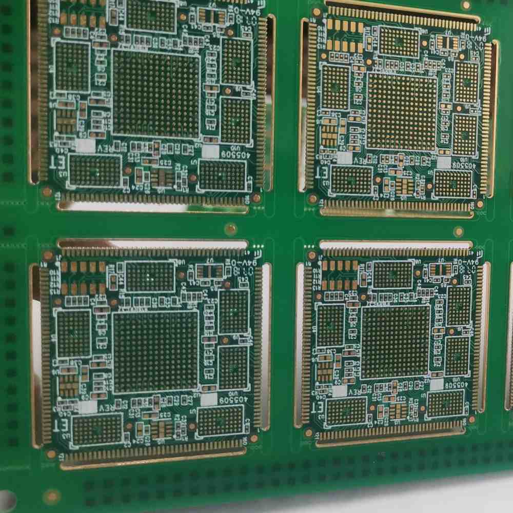
The dielectric materials used in HDI fabrication are specialized laminates engineered to enable the fine features, withstand the demanding processing conditions required, and deliver stable electrical performance. Typical materials for HDI include:
Polyimides
Polyimides like HD-4000 from Hitachi or Durimide from Rogers offer thermoset polymers with excellent dimensional stability after curing and at higher temperatures. This makes them suited for the repeated lamination cycles in sequential build HDI processing. They have lower loss than traditional FR-4 material.
High Tg Epoxies:
Materials such as Nelco 4000-13SI have high glass transition temperatures above 170°C. This provides good thermal resistance when building up successive dielectric layers. These epoxies still absorb more moisture than polyimides though.
PTFE Blends:
Blends of PTFE (polytetrafluoroethylene) and epoxy provide a balance of dimensional stability and low loss performance. Rogers RO4350B is a common example containing a PTFE filler. The PTFE contributes a lower dielectric constant and loss tangent.
Liquid Photoimageable Dielectrics (LPID):
LPIDs like Taiyo PSR-4000 AUS are epoxy based resins that can be screen printed then photocured. They enable fine features with tight alignment between layers, ideal for high density stacking. But they require extra process steps.
Selecting the right materials is key to achieving reliable HDI designs. This includes properly matching material properties and coefficients of thermal expansion between dielectrics, cores, and copper.
Key Manufacturing Processes in HDI
While HDI fabrication leverages many standard PCB processing methods, the technology also requires some unique and specialized manufacturing techniques.
Laser Drilling
Laser drilling using Nd:YAG lasers is typically required to produce the 3-5 mil diameter microvias in HDI with the accuracy and precision needed. Mechanical drilling cannot reliably reach these microvia dimensions. Lasers also generate less stress on low loss dielectric material compared to standard drill bits.
Build-Up Layer Processing
Semi-additive processing is implemented to fabricate the fine traces in HDI build-up layers. A thin seed copper layer is first deposited over the dielectric. Photoresist is then lithographically patterned and developed to form the trace images. Copper is electroplated to build up the traces before etching away unwanted areas.
Sequential Lamination
Coreless HDI structures utilize sequential lamination where dielectric and copper foil layers are built up one at a time. Each layer is fully imaged, etched, inspected, and treated before the next layer is added. Dielectrics must be properly treated to promote reliable adhesion between layers during repeated lamination cycles.
Registration
Maintaining tight layer-to-layer registration is critical with microvias and fine features. Tight controls over material shrinkage, lamination pressures, and imaging processes are implemented to hold alignments within 1 mil or better. Automated optical inspection helps verify registration.
Surface Finishes
OSP and immersion silver are common final finishes used with HDI PCBs. They protect the thin, dense copper traces from oxidation and whiskering. ENIG or ENEPIG may also be used but can present plating challenges with smaller features.
HDI Testing and Inspection
While essential for functionality and reliability, testing and inspection of HDI boards also presents challenges due to the small feature sizes and tight tolerances involved.
Electrical Testing (ICT and Flying Probe)
HDI designs require test fixtures with fine pitch probes and safe actuation pressures. ICT with micro-spring probes can handle high densities. Grid array probes for flying probe testers are also available with pitches below 10 mils.
Automated Optical Inspection (AOI)
Most HDI facilities utilize automated optical inspection upstream and downstream of key process steps. AOI can validate microvia dimensions, trace sizes, layer alignments and detect potential defects. Specialized algorithms and pattern recognition processing are utilized to handle the high density image analysis.
Microsectioning
Detailed cross-sectioning and inspection of microvias, interfaces, and connections under microscope validates quality. Sectioning equipment with micrometer precision alignment and diamond saw blades facilitate cutting HDI coupons for analysis.
X-Ray Inspection
X-ray imaging allows inspection of microvia fill and plating quality without requiring microsectioning. It is a common technique for verifying the presence of reliable copper plating through stacked microvias which cannot be analyzed from external visual inspection alone.
HDI Design Software Tools
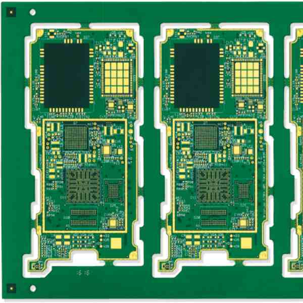
To effectively design and layout boards utilzing HDI technology, EDA software tools are required that provide the capabilities to create and validate complex HDI routing.
Layout Routing
Advanced PCB layout tools like Mentor Xpedition, Cadence Allegro, and Altium Designer incorporate specialized features to facilitate HDI routing like:
- Configurable design rule checking down to 4 mil traces/spaces
- Microvia and stacked via integration
- Automated impedance tuning tools
- Real-time DFM feedback and collision warnings
- Length matching utilities
- 3D field solver integration
Signal Integrity Simulation
Tools such as Ansys SIwave, Mentor HyperLynx, and Cadence Sigrity are used to simulate signal performance. This verifies proper impedance control, analyze coupling risks, and predict signal waveforms through the HDI structure.
Thermal Modeling
Understanding temperature profiles and thermal stresses is critical in HDI designs. FEA modeling using tools like Ansys Icepak or Mentor FloTHERM help predict hot spots and reliability risks.
DFM Analysis
Design for manufacturing tools analyze designs versus fabrication capabilities to avoid producibility issues and predict yields. These are especially valuable in HDI to assess challenges with microvias, traces, and tolerances.
Applications of HDI Technology
Some of the key product applications benefiting from HDI PCB technology include:
Smartphones
HDI allows smartphones to integrate more features and performance in thinner and more compact form factors demanded by users. The technology will continue playing a key role with emerging flexible smartphones as well.
Wearable Technology
With miniaturization requirements even greater than mobile phones, wearable products like smart watches rely extensively on HDI to achieve the necessary component integration and circuit density.
Internet of Things (IoT)
As internet-connected sensors and devices proliferate, HDI fabrication techniques facilitate the tiny, high reliability PCBs needed for these applications to function.
Tablets/Laptops
Portable consumer electronics require maximum functionality and battery life in limited space. HDI allows these devices to pack more computing power through greater circuit density.
Automotive Electronics
HDI provides a solution for adding intelligence and connectivity to automotive systems while meeting ruggedness and reliability requirements. Driver assist and EV systems are prime examples.
Medical Electronics
Implantable and wearable medical devices demand increased capabilities along with biocompatible, compact packaging. HDI integration is key for delivering these advances in medical technology reliably.
The Future of HDI Technology
HDI fabrication processes and materials will continue evolving, enabling finer features and higher component densities. Some key developments on the horizon include:
- Microvias below 3 mils enabling further miniaturization
- Improved reliability of microvias for longer product life cycles
- Extending HDI structuring to additional flex and rigid-flex designs
- Increased mainstream adoption beyond high-end applications
- Tighter registration capabilities below 0.5 mils
- Advanced and lower loss dielectric materials
- Improved thermal management techniques
- Innovation of inspection techniques for verifying tighter geometries
- Development of thermal and mechanical finite element modeling
- Expansion of HDI and microvia utilization to higher power
As the demands for sophisticated portable electronics grow, HDI fabrication will be pushed to new limits using both evolutionary and revolutionary approaches. This will position PCB technology to continue enabling the electronics innovations of the future.
Frequently Asked Questions
What are the typical cost differences between HDI and standard PCBs?
In general, HDI fabrication can increase costs by 20-40% over standard multilayer boards due to the more complex processing, materials, and lower yields involved. However, by utilizing HDI technology to reduce layer counts in a design, the cost premium can usually be minimized.
At what layer count does it make sense to transition to an HDI design?
A typical threshold for considering HDI is once a board layer count reaches 12-16 layers. The reduced layer requirements of HDI often offsets its higher costs at these layer quantities.
What are some key reliability concerns with HDI boards?
Major reliability risks center around the microvias, including cracking, fracturing, and delamination around low aspect ratio vias. This is mitigated following proper HDI design rules. Warpage can also be a concern with some ultra-thin coreless HDI constructions.
What are the limitations on traces and spaces with HDI technology?
While features down to 2 mils are possible with HDI, typical minimum practical trace/space is around 4 mils for manufacturability. The thinnest traces may require thicker copper to avoid resistance or reliability issues.
Can microvias be repaired and filled if defects are found?
If needed, blind microvias can be plugged using copper electroplating or specialty liquid inks. But this increases process complexity and cost. Microvia reliability should be designed in from the start.
Conclusion
HDI offers transformative advantages for electronics by enabling integration of complex, high performance circuits in extremely compact form
Leave a Reply