Introduction
HDI (High-Density Interconnect) printed circuit boards (PCBs) have become increasingly important in recent years for their ability to accommodate high component densities and enable shrinking electronic devices. As electronics continue getting smaller, lighter, and more powerful, HDI PCBs provide the interconnect solution to fit more functionality into less space.
This guide will provide a comprehensive overview of HDI PCB technology, including what sets it apart from standard PCBs, key manufacturing processes and design considerations, application areas where HDI shines, and future trends. With electronics innovation showing no signs of slowing down, understanding HDI PCB capabilities is crucial for PCB designers, manufacturers, and OEMs that need to stay on the cutting edge.
What Are HDI Printed Circuit Boards?
HDI PCBs can be distinguished from conventional PCB technologies by their use of microvias—tiny vias with diameters less than 150 μm (microns). Whereas standard PCBs rely on vias with 200 μm diameters or larger, HDI PCBs utilize laser drilling techniques to achieve microvia holes with diameters down to just 50 μm.
These miniscule microvias enable trace pitches and line/space widths down to 30-50 μm, supporting component densities up to 20 times greater than conventional PCBs. Stacked microvias also allow connections between multiple board layers with less surface area than drilling each layer conventionally.
Other key characteristics of HDI PCB technology include:
- More than 6 layers, often >10 layers
- Thin dielectric buildup layers, as low as 25 μm
- Fine line traces/spaces down to ≤50 μm
- High interconnect density >300,000 holes/m2
- Microvias with ≤150 μm diameters, enabling stacked vias
- High-frequency support up to >3 GHz
- Improved signal integrity from tightly coupled power/ground
- Thin overall board thickness ≤1.6 mm
- Laser drilling for precision microvias
By combining ultra-dense microvias, fine circuitry, and thin dielectric layers, HDI PCBs achieve the miniaturization and performance not attainable with conventional PCBs. This enables far greater functionality in products where small size and high speeds are critical.
Advantages of Using HDI PCBs
Here are some of the top advantages HDI PCB technology provides compared to standard PCBs:
- Higher component density – Microvias allow 3-5x more components to be placed per unit area
- Miniaturization – HDI PCBs can achieve up to 70% reduction in area versus conventional designs
- Layer reduction – By utilizing stacked microvias, fewer layers are needed to interconnect components
- Signal integrity – Shorter traces, closely spaced power/ground, and stacked vias minimize noise and crosstalk
- High-frequency support – Thin dielectrics and fine geometries support multi-GHz frequencies
- Finer pitches – Enables 0.4 mm BGA packages and 0.3 mm pitch QFNs and other fine-pitch components
- Lower costs – Despite higher fabrication costs, total system cost is lower through miniaturization
- Improved reliability – Microvias provide redundant connections eliminating hairline cracks
For advanced PCBs where size, speed, and reliability are prime concerns, HDI technology provides tangible advantages over standard PCB processes. The tradeoff is higher fabrication complexity and cost, which is justified for leading-edge products.
HDI PCB Design Considerations
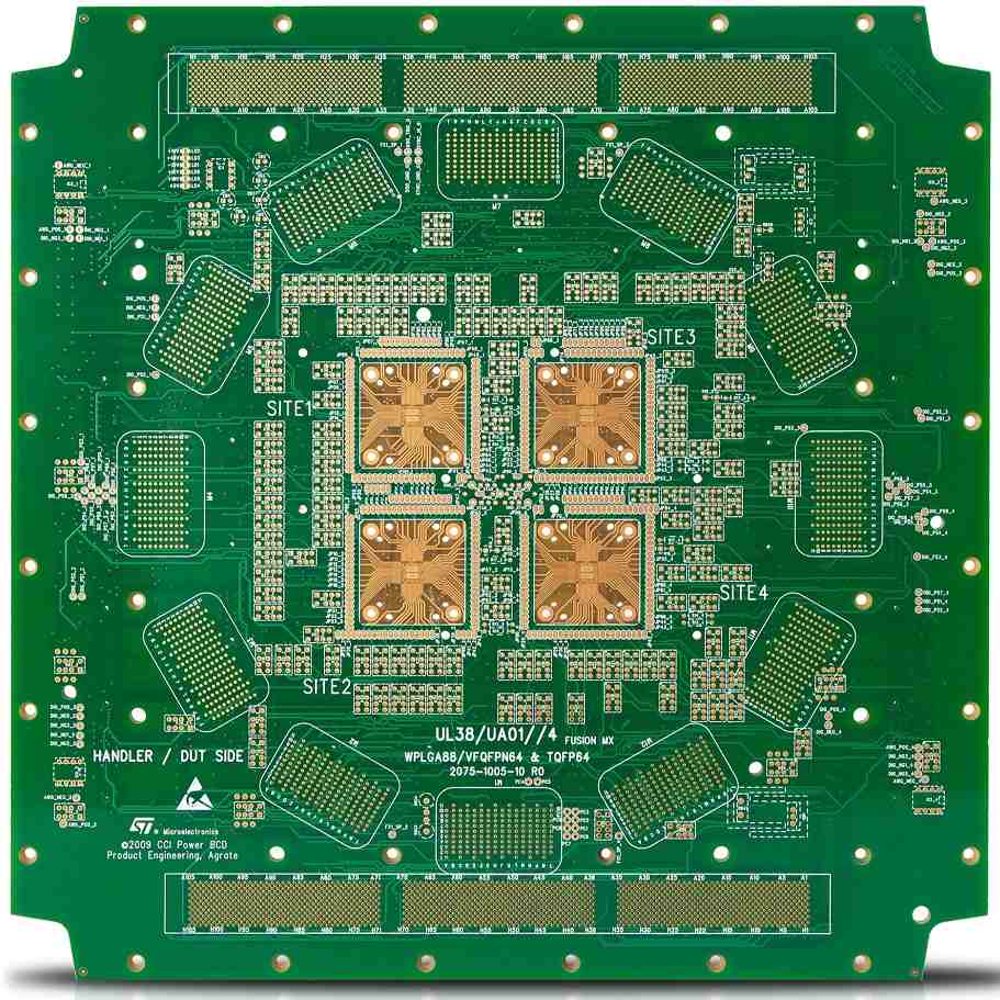
Designing a high-performance HDI PCB requires special considerations to utilize the technology most effectively while avoiding pitfalls. Here are some key HDI PCB design guidelines:
Layer Stackup
The layer stackup defines the layer structure of the PCB including the number of layers, order, and dielectric materials used. For HDI, typical stackups use 6 to 12 conductive layers. This enables integrating dense microvias between layers while reserving enough layers for dense circuit routing. Common configurations include:
- 6-layer – Well balanced performance/cost compromise
- 8-layer – Enables higher speeds and densities
- 10-layer – Ideal for advanced applications with max density
- 12-layer – Highest performance but diminishing returns on additional layers
The stackup alternates conductive layers with insulating dielectric materials. Common thicknesses range from 35 μm to 70 μm for the thin high-speed dielectric layers up to 150 μm for thicker outer layers. Choosing dielectrics with tight thickness and tolerance control minimizes impedance discontinuities.
Microvia Strategies
A primary advantage of HDI technology is the use of microvias for vertical connections through the PCB. However, care must be taken in their implementation:
- Minimize stub lengths by placing surface pads directly over microvias
- Use stacked/staggered microvias for redundancy and improved connection reliability
- Balance microvia pad sizes – larger than finished drill size but small enough to allow high densities
- Limit the number of successive microvia layers to control via stress and formation challenges
- Utilize capture pads on inner layers for reliable connections to microvias
By carefully designing microvia layouts and sizes, reliable interconnects can be achieved.
Controlled Impedance Routing
For high-speed signals, controlled impedance traces matched to the impedance of components is mandatory. This requires proper stackup materials selection and trace geometry tuning:
- Use impedance calculators to determine trace width/spacing for target impedance (generally 50-100 ohms)
- Tightly control dielectric material thickness and consistency to maintain impedance
- Minimize length of uncontrolled impedance traces such as vias
- Allow for wider power/ground traces to minimize impedance changes from edge coupling
Matching PCB traces to component impedances maximizes signal integrity and efficiency at high frequencies.
Power Distribution
Carefully planning power distribution prevents voltage drops and noise:
- Use multiple power and ground pairs placed close together for decoupling
- Incorporate power planes whenever possible for lowest impedance supply routing
- Provide multiple vias when transitioning power between layers
- Utilize capacitors for decoupling directly adjacent to integrated circuits
Proper PCB power distribution design is especially crucial given HDI’s high component density.
Thermal Management
With HDI’s dense component packing, thermal heat dissipation demands attention:
- Use thermal vias/pads under hot components to conduct heat to internal layers or bottom layer
- Incorporate metal core or thick copper layers to spread heat laterally
- Allow adequate airflow for cooling or holes for supplemental fans
- Use thermally conductive dielectric materials when suitable
- Limit component heat sources and distribute them when possible
Careful thermal analysis should guide HDI designs to prevent overheating.
By following sound design principles tailored to HDI PCB capabilities and limitations, high performing and reliable systems can be achieved.
HDI PCB Fabrication and Materials
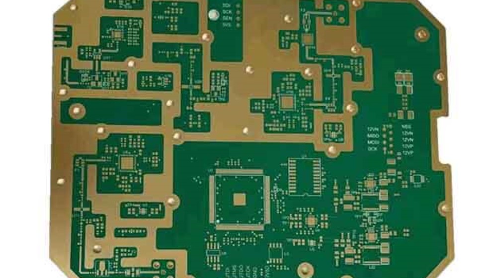
Fabricating HDI PCBs requires specialized processes and materials to achieve the tight tolerances and high interconnect densities. Here are some of the unique fabrication aspects of HDI PCB production:
Layer Dielectrics
To attain the thinnest dielectric layers required, KAPTON-based films as thin as 25 μm are commonly used along with glass reinforced materials like FR4 as thin as 35 μm. The ultra-thin KAPTON layers provide:
- Excellent thickness tolerance control
- Low and stable dielectric constant
- High tensile strength despite thinness
- Good thermal resistance for inner layer stability
Well-controlled dielectrics enable impedances and performance predictability.
Laser Drilling
To achieve the small microvias required, mechanical drilling is replaced by laser drilling. This provides smaller and higher precision holes including:
- Diameters down to 50 μm vs. 150 μm for mechanical drilling
- Tight diameter tolerances within +/- 10 μm
- High accuracy locations +/- 25 μm
- Ability to taper holes for improved plating adhesion
- Minimal smear and damage of dielectric layers
Laser drilling is essential for creating ultra-dense stacked microvias.
Plating Processes
HDI PCBs integrate a series of plating processes to reliably plate the microvias and circuits:
- Plasma etching cleans and micro-etches surfaces for improved plating adhesion
- Electroless copper provides thin starter plating for uniform plating foundation
- Microvia filling using copper electroplating builds up copper thickness from within the microvias outwards
- Panel plating uniformly deposits copper across the entire panel to limit thickness variations
- Flash plating lays quick copper to enable etching fine traces
Advanced plating processes allow reliably interconnecting high densities of microvias.
Final Finishes
HDI designs use thinner copper (15-20 μm) to enable fine L/S traces. Final finishes protect these thinner cu tracts:
- Electroless nickel immersion gold (ENIG) provides excellent shelf life and solderability
- Organic solderability preservatives (OSPs) are lower cost but have shorter shelf life
- Gold plating provides the highest performance for specialized applications
Proper surface finishes maximize the lifecycle of thin HDI copper traces.
While fabricating HDI PCBs is challenging, the right processes and materials help realize the technology’s advantages.
HDI PCB Applications
With its abilities to create highly compact and high-speed PCBs, HDI technology is used across a range of advanced electronics:
Consumer Electronics
Smartphones, wearables, tablets, and notebooks must integrate maximum functionality into extremely compact and lightweight packages. HDI PCBs enable these feats of miniaturization required.
Internet of Things (IoT)
Networked sensors, controls, and electronics need strong signal integrity and noise control in dense and low power designs ideal for HDI PCBs.
Automotive Electronics
Advanced driver assistance systems (ADAS), infotainment, and control systems use HDI PCBs for their safety, performance, and reliability.
High-Speed Communications
Networking switches, routers, servers, and telecom rely on HDI PCBs to provide high densities of multi-GHz components and interconnections.
Aerospace and Defense
Mission-critical electronics need rugged HDI PCBs that maximize reliability in high vibration, shock, and temperature environments.
With its unmatched interconnect density, HDI continues growing across electronics sectors where performance and reliability are paramount.
The Future of HDI Technology
While HDI PCBs represent the pinnacle of PCB technology today, development continues to push HDI fabrication and design limits even further. Here are some trajectories where continued HDI PCB evolution is occurring:
- Finer features – Traces and spaces keep shrinking, targeting ≤25 μm widths. Microvias likewise keep getting smaller with ≤25 μm diameters.
- More layers – Layer counts increase for greater densities, with high-end designs moving to 14 layers and beyond.
- Advanced materials – Dielectrics with lower dielectric constants and loss tangents enhance high-frequency performance.
- Improved design integration – Tighter coordination of electrical, thermal, and mechanical design ensure reliability.
- Expanded applications – HDI usage grows from high-end electronics into mainstream commercial markets.
- Improved modeling – More accurate modeling and analysis reduces over-design margins.
- Additive processing – Additive semi-additive processes replace etching to attain smaller features.
HDI PCB technology will continue advancing to integrate ever-denser functionality in smaller and faster systems.
Conclusion
HDI PCB fabrication represents the leading edge of printed circuit board technology evolution. The combina
Frequently Asked Questions
What are the key advantages of HDI PCBs compared to standard PCBs?
Some of the main benefits HDI PCBs provide over conventional PCBs include:
- Higher component density through microvias
- Enabling miniaturization of electronics
- Supporting higher speeds and frequencies
- Improved signal integrity from tightly spaced power/ground
- Lower overall system cost despite higher PCB cost
- Greater reliability through redundant connections
HDI PCBs deliver size, performance, and reliability gains where conventional PCBs hit limitations.
What minimum microvia diameter can HDI PCBs achieve?
With laser drilling techniques, HDI PCB microvias can be fabricated with diameters down to 50 microns (μm). This allows much smaller vias than the 150 μm minimum diameter typical for mechanically drilled vias on standard PCBs.
How many HDI PCB board layers are typical?
Most HDI designs utilize stackups ranging from 6 to 12 layers. Having at least 6 layers provides good versatility with microvias while limiting complexity. 12 layers approaches the maximum density capability, but can increase costs without substantial gains over 8-10 layer HDI stackups for most applications.
What are some key HDI PCB design guidelines?
Critical HDI PCB design considerations include:
- Proper layer stackup and dielectric selections
- Optimized microvia layouts and sizes
- Controlled impedance routing for high frequencies
- Solid power distribution network
- Thermal analysis and management
- Following fabrication and assembly capabilities and tolerances
Paying attention to these areas helps maximize HDI PCB performance and manufacturability.
What types of electronics benefit most from HDI PCB technology?
Some products that gain substantial advantages from HDI PCB capabilities include:
- Consumer electronics like smartphones seeking miniaturization
- High density, high speed networking and communications equipment
- Cutting edge aerospace and defense electronics
- Advanced driver assistance systems (ADAS) for automotive
- IoT devices needing small size and high reliability
HDI PCBs deliver interconnect density and signal integrity gains very useful across complex, compact, and high performance electronics.
Leave a Reply