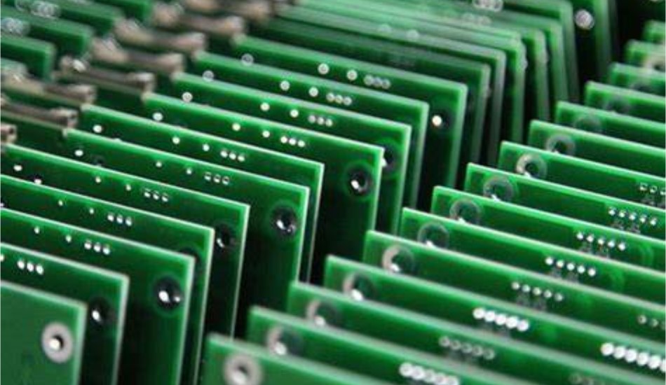
As electronics become smaller and more complex, the demand for high density interconnect (HDI) printed circuit boards (PCBs) has increased significantly. HDI PCBs allow for tighter spacing and smaller components than standard PCBs by using microvias to connect multiple board layers. This enables more functionality to be packed into a smaller space.
Choosing the right HDI PCB manufacturer is crucial to get boards fabricated correctly for your application. With so many suppliers to pick from, it can be daunting to select one that meets your specific needs. This article provides an in-depth guide on what to look for when selecting an HDI PCB supplier and the key factors to consider.
What is HDI PCB Technology?
HDI stands for high density interconnect or high density interconnection. It refers to PCBs that have a higher component density than conventional PCBs.
Some key characteristics of HDI PCBs:
- Tighter spacing between conductors and components down to 25um or less
- Microvias with diameters less than 150um connecting layers
- Thinner copper layers down to 1 or 2um thick
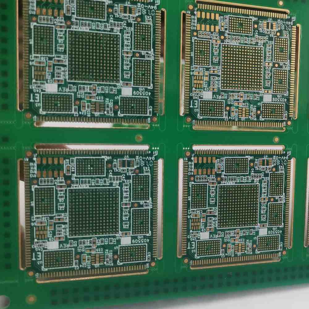
- More layers – typically 6 to 12
- Fine line traces and spaces less than 100um
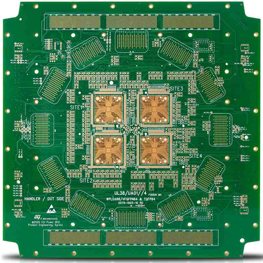
HDI technology allows routing high density surface mount components like BGAs, CSPs, 0201 and 01005 passives in a compact form factor. It provides design flexibility to integrate more functionality in same space.
HDI PCBs enable miniaturization and increased performance for advanced electronics used in consumer mobile devices, wearables, IoT devices, medical devices, aerospace and automobile electronics.
Benefits of Using HDI PCBs
Here are some of the main benefits of using HDI printed circuit boards:
Increased Routing Density
The main advantage of HDI PCBs is the ability to route traces much more tightly without compromising on signal integrity. Microvias also reduce the need for traces to change layers. This facilitates routing high pin count components in a small form factor.
Miniaturization
HDI technology allows for greater component density, thus enabling product miniaturization. More functionality and components can be fit into a compact space ideal for small handheld consumer electronics.
Improved Electrical Performance
Thinner dielectric materials and precise trace dimensions enhance signal speed, clarity and impedance control. This improves overall electrical performance.
Layer Count Reduction
By using microvias, HDI PCBs can achieve higher routing density with fewer layers. A 6 layer HDI board can replace a 12 layer conventional PCB with equivalent routing capabilities. This reduces costs.
Better Heat Dissipation
The laminate materials used in HDI boards have a lower thermal resistance allowing heat to dissipate faster. This enhances the thermal management of boards with high power components.
Lower Weight
With fewer layers and thinner dielectrics/conductors, HDI PCBs weigh less than conventional PCBs. This lightweight advantage suits aerospace and satellite applications.
Design Flexibility
HDI processing offers more freedom and flexibility to PCB designers. Components can be placed more optimally. Microvia technology enables connections from any layer to any other layer for unrestricted routing.
HDI PCB Fabrication Process Overview
Here is a brief overview of the HDI PCB fabrication process and how it differs from standard PCB manufacturing:
- HDI processing requires specialized materials – dielectric laminates, prepregs and copper foils. These enable the fabrication of thinner layers and traces.
- Laser drilling forms microvias instead of mechanical drilling. Laser drills produce small diameter holes with high accuracy ideal for HDI boards.
- Plating of microvias and traces involves conformal copper deposition to metallize the holes and build up circuit layers.
- Additional lamination steps are incorporated to stack and bond the thin dielectric and circuit layers together into a multilayer board.
- PCB imaging uses a laser direct imaging (LDI) process capable of resolving fine line geometries down to 25um or less.
- Etching, stripping and other processes require tight process controls to maintain the integrity of thin features throughout fabrication.
- Electrical testing methodology differs to test HDI boards using flying probe or ICT testers suitable for verifying high density microcomponents.
- Automated optical inspection (AOI) during assembly checks for defects at multiple process stages including post-soldering.
There are several key differences from conventional PCB manufacturing. HDI PCB fabrication demands advanced materials, specialized equipment, tight process controls and inspection methods to reliably produce these high precision boards.
Factors to Consider When Selecting an HDI PCB Manufacturer

Choosing a reliable HDI PCB supplier requires evaluating a range of factors from their capabilities and experience to service quality.
Here are some important considerations when selecting an HDI PCB manufacturer:
Technical Capability
- Examine their HDI technology – are microvias and trace spacing below 150um and 100um respectively? Do they use advanced dielectric materials compatible with HDI?
- Laser drilling capability – UV laser is ideal for drilling microvias. Mechanical drilling limits via sizes above 150um.
- Layer stackup knowledge – can they recommend optimal stackups? Model electrical performance?
- Engineering support – can they design manufacturable HDI boards compliant with your requirements?
- Reliable processes – do they implement statistical process controls to ensure repeatable quality?
- Quality certifications – IPC and AS9100 certifications demonstrate standardized quality systems.
HDI Experience
- Number of years manufacturing HDI PCBs – longer experience means refined expertise.
- Types of HDI applications catered to – diverse experience suits complex, high mix boards.
- Volume production capacity – can they handle your ongoing production needs?
- Engineering depth – do they have resources to debug and optimize HDI designs?
- Understanding of design challenges – will they provide layout tips and stackup advice?
Range of HDI Services
- Design support – offering layout reviews, stackup design, signal integrity analysis.
- Quickturn prototyping – fast quoting, fabrication and assembly for quick HDI prototyping builds.
- Volume production – consistent quality across low to high volume batches.
- Turnkey assembly – in-house assembly with fine pitch component capabilities.
-Testing services – full electrical and functional testing options.
-Post-sales support – prompt assistance with technical queries, optimization, failure analysis.
Quality and Delivery
- Quality metrics – yield rates, defect rates reveal process capability.
- On-time delivery – can they meet your timelines with good inventory management?
- Quality certifications – ISO, IPC, AS9100 certification indicates standardized quality.
- Risk management – business continuity plan for production assurance.
- Supply chain management – diverse approved vendor lists ensure material availability.
- Documentation – detailed travelers, statistical reports show process control.
Customer Service
- Technical expertise – can they understand your specific requirements?
- Design support – will they help optimize designs for manufacturability?
- Communication – do they respond promptly to inquiries and updates?
- Business transparency – are pricing, lead times, and payments clear?
- Continuous improvement – do they implement feedback and drive innovation?
Select an HDI PCB partner focused on solving your challenges through engineering collaboration and manufacturing excellence.
Questions to Ask Prospective HDI PCB Manufacturers
Here are some key questions to ask HDI PCB suppliers before selecting one:
- What HDI materials and stackups do you offer? Can you handle flexible HDI circuits?
- What is your microvia and trace/space capability? How small can you reliably produce?
- Do you have in-house laser drilling? What size microvias can you drill?
- How do you metallize and plate microvias? Electroless or direct plating?
- What laminating process do you use? Do you have vacuum lamination?
- What is your minimum finished hole size for components after plating?
- Can you direct image traces below 100 microns? What is yourminimum linewidth?
- How do you inspect HDI boards during fabrication and assembly?
- What electrical test capabilities do you have for verifying HDI boards?
- What statistical process controls do you implement for quality assurance?
- Can you provide HDI design guidelines and stackup recommendations?
- How do you qualify and control your material supply chain?
- What engineering resources can you provide during HDI design?
- Can you assess signal integrity issues and provide modeling?
- What test vehicles and coupons do you use to qualify HDI processes?
- How do you package and ship fragile HDI boards?
- What support do you provide if there are any quality issues?
Their responses will help reveal process capabilities, experience, expertise and service quality.
Red Flags to Watch Out for When Selecting an HDI PCB Supplier
While evaluating HDI PCB manufacturers, look out for these red flags which may indicate risk:
- No microvia drilling capability – This forces reliance on mechanical drilling with larger via sizes.
- Limited layer count ability – Good HDI suppliers can produce high layer count boards (>10 layers)
- Only offering basic materials – Lack of high performance laminates may restrict electrical capabilities.
- Poor communication – Long delays in responding to inquiries or providing feedback.
- Outdated website – Indicates limited investment in technology and equipment.
- Unable to provide HDI design guidelines – Lack of expertise to support complex HDI designs.
- No quality certifications – IPC and ISO certs provide assurance of standardized quality systems.
- No in-house assembly – Important for assembling fine pitch HDI boards without damage.
- Unclear pricing – Avoid firms unwilling to provide clear quotes or sample pricing.
- Cannot handle quickturn – Good HDI suppliers have fast prototyping capabilities.
- Lack of customer testimonials – Look for positive customer reviews of service quality.
- Unable to provide HDI process data – Legitimate suppliers will share test coupon data, etc.
Watch for these red flags when evaluating HDI PCB manufacturers to avoid choosing a supplier unable to meet your requirements.
Leading HDI PCB Manufacturers
Here are some of the leading global HDI PCB manufacturers to consider:
TTM Technologies
One of the top HDI PCB producers offering quickturn prototyping and high volume production globally.
HDI Capability: Laser microvias down to 75um, traces/spaces to 3/3 mils, 16+ layers.
Services: Quickturn, engineering support, RF applications.
Industry Segments: Aerospace, medical, computing, networking, telecom.
AT&S
European firm focused on high-end HDI, rigid-flex, metal core PCBs for automotive and medical customers.
HDI Capability: Laser microvias to 60um, spaces under 4 mils, 16 layer.
Services: Prototyping, rigorous testing, HDI design.
Industry Segments: Automotive, medical, industrial, aerospace.
Compeq
Taiwanese manufacturer providing HDI PCBs from quickturn prototyping to mass production.
HDI Capability: Microvias to 8 mils, 4 mil lines/spaces, 20 layers.
Services: Design, quickturn, RF boards, flex and rigid-flex.
Industry Segments: Communications, consumer, automotive, IoT.
Unimicron
One of Asia’s leading manufacturers capable of advanced HDI and substrate technologies.
HDI Capability: Laser microvias to 60um, 3/3 mil lines/spaces, 16 layers.
Services: HDI design, quickturn, RF, flex, rigid-flex PCBs.
Industry Segments: Automotive, telecom, consumer, medical.
Tripod Technology
Taiwanese firm offering advanced HDI capabilities combined with turnkey assembly services.
HDI Capability: Laser microvias to 75um, 2/2 mils lines/spaces.
Services: Turnkey PCB assembly, design, quickturn, flex/rigid-flex.
Industry Segments: Communications, computing, consumer, automotive.
There are many capable HDI PCB manufacturers across North America, Europe and Asia. Evaluate suppliers against your specific requirements.
Key Takeaways on Selecting an HDI PCB Manufacturer
- Check technical capabilities – microvia sizes, trace widths, layer counts, material expertise.
- Assess their experience producing diverse, complex HDI boards over many years.
- Look for comprehensive design support – stackup recommendations, modeling, layout reviews.
- Verify their quality management – certifications, process controls, test methods.
- Examine breadth of services – engineering, quickturn, assembly, testing, analysis.
- Require evidence of consistent on-time delivery and high yields.
- Select a responsive partner willing to collaborate on optimizing your design.
Choose an HDI PCB supplier with proven expertise that matches your prototyping and production needs.
Frequently Asked Questions
What are some common applications of HDI PCBs?
Some common applications are:
- Smartphones and tablets
- Laptops, PCs and servers
- Networking and telecom hardware
- Automotive electronics
- IoT and wearable devices
- Medical devices
- Military and aerospace avionics
How are microvias formed in HDI PCB fabrication?
Microvias are formed by laser drilling which can drill small diameter holes down to 50-75um (2-3 mils). The holes are then plated with an electroless copper process to metallize the hole walls prior to copper plating.
Can flex PCBs be manufactured in HDI technology?
Yes, flex PCBs using polyimide dielectric films can be fabricated in HDI technology. This includes multilayer flex circuits as well as rigid-flex boards. However, flex PCBs require specialized handling during fabrication.
What design principles should be followed for HDI PCBs?
Some HDI design guidelines include:
- Minimize unnecessary layer changes through careful routing
- Place components on outer layers for shortest routing to microvias
- Limit trace length differences to match electrical lengths
- Use 45° traces between microvias for smoother current flow
- Group components with high frequency signals for isolation
What panel sizes do HDI PCB manufacturers normally support?
Many HDI PCB suppliers can manufacture panel sizes up to about 18″ x 24″ (457mm x 609mm). However, some manufacturers support larger panel sizes. Maximum panel size depends on equipment constraints.
Are there limitations on the component pin pitch for HDI PCB assembly?
The microvia sizes and thin dielectric layers used in HDI enable assembling very fine pitch components. 008004 inch (0.2mm) pitch BGAs and 01005 passives can be reliably assembled on HDI boards.
Conclusion
HDI PCB technology enables the miniaturization and performance essential for contemporary electronics through high density routing, thinner layers, microvias and fine features. However, realizing the benefits of HDI requires selecting the right PCB manufacturer.
Choose an HDI supplier with in-depth experience, advanced process capabilities, rigorous quality systems, comprehensive services, and close customer collaboration. Evaluating manufacturers against key criteria will help identify the ideal HDI partner to fulfill your current and future PCB requirements. Partnering with a tier one HDI PCB producer will ensure you get boards fabricated correctly with the technology optimized for your application needs.


Leave a Reply