Introduction
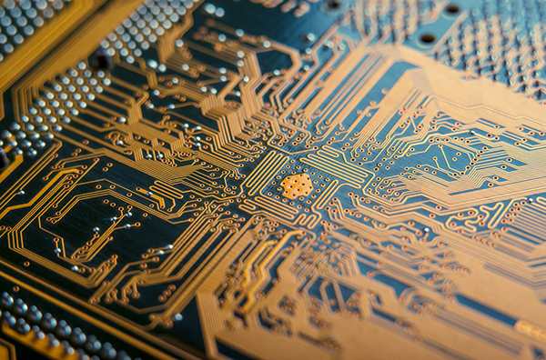
HDI (High Density Interconnect) PCBs (Printed Circuit Boards) are an advanced type of PCB that allows for higher component density and more complex circuitry than standard PCBs. HDI technology enables the fabrication of boards with extremely fine traces and spaces, smaller vias, and higher connection pad densities. This allows packing more functionality into a smaller space while maintaining high reliability.
The HDI manufacturing process integrates several advanced PCB fabrication techniques to achieve the high density and performance required. This includes processes like laser direct imaging (LDI) for very fine trace/space capability, microvia formation to connect layers, and often the use of thinner dielectric materials.
In this comprehensive guide, we’ll cover:
- Overview of HDI PCB technology
- HDI PCB design and layout considerations
- Step-by-step HDI PCB fabrication process
- HDI testing and quality control
- HDI PCB applications
- Comparison to standard PCB manufacturing
- Benefits and challenges of HDI PCBs
Let’s get started understanding the complete manufacturing process behind these advanced boards.
Overview of HDI PCB Technology
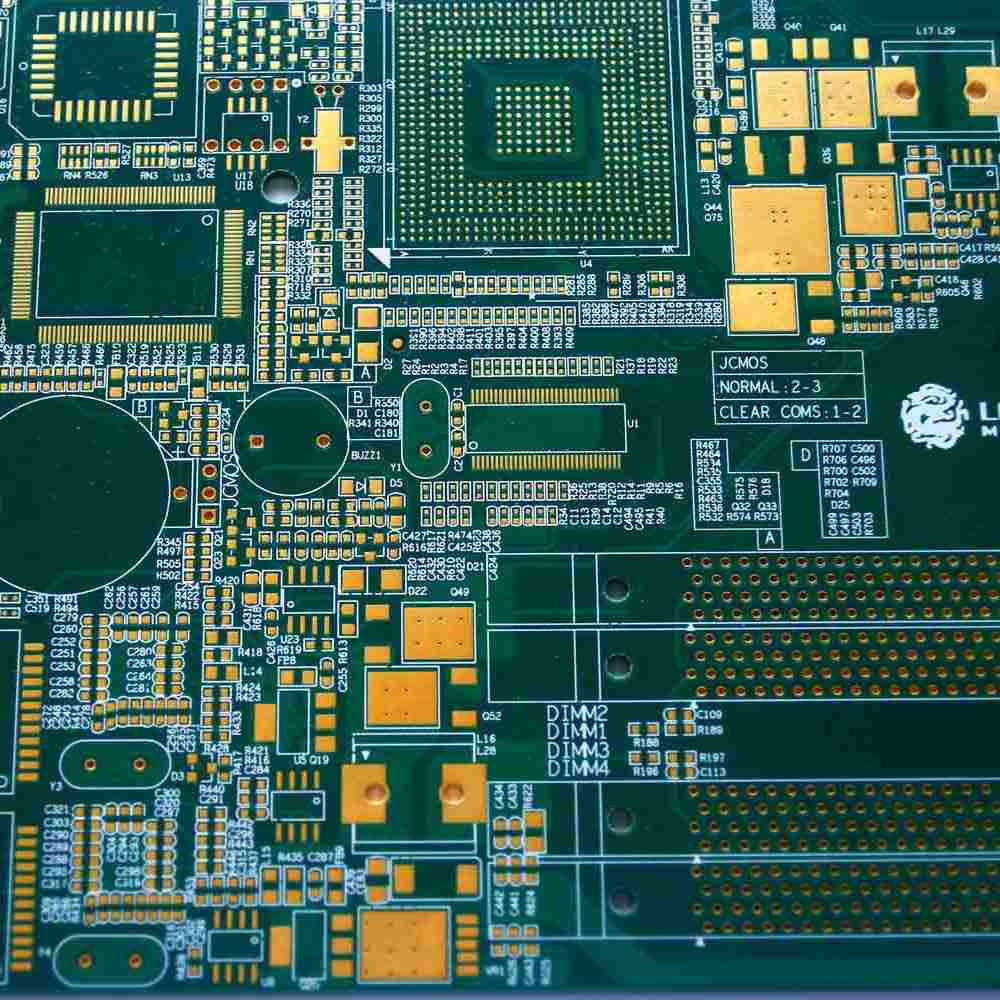
HDI PCBs first emerged in the 1980s to meet growing demands for miniaturization and performance in electronics packaging for defense, aerospace, and computing applications. Since then, HDI technology has continued advancing and is now widely used in consumer electronics like smartphones and tablets.
Some key characteristics of HDI PCB technology include:
- Fine line/space capability down to 15μm or below
- Microvias with diameters below 150μm connecting layers
- Thinner dielectric buildup layers (25-50μm)
- Higher connection pad densities (>20 pads/mm2)
- Layer count >6 layers
- Often incorporate blind and buried vias
- Allows 3x to 5x increase in circuit density vs. conventional PCBs
To achieve these high densities, HDI PCB fabrication integrates a number of advanced processes:
Laser Direct Imaging (LDI)
LDI machines use a laser to image traces directly onto photosensitive layers of the PCB without using a physical mask. This eliminates alignment issues and allows imaging of extremely fine features down to 15μm or below.
Microvia Formation
Microvias with diameters below 150μm are drilled with advanced techniques like laser or plasma etching to interconnect board layers. This allows high-density interconnections.
Thin Dielectrics
Thinner dielectric buildup layers (25-50μm) are deposited, enabling tighter trace/space and closer layer stacking.
Sequential Buildup
Dielectric and copper layers are added one at a time (sequentially built up), providing design flexibility.
These advanced fabrication processes enable the high circuit densities, fine features, and advanced packaging capabilities of HDI PCBs. However, they also introduce manufacturing challenges that require specialized processes and strict process control.
HDI PCB Design and Layout
Before fabrication, HDI PCBs require careful design and layout practices to ensure manufacturability and performance. Here are some key guidelines:
- Account for fabrication tolerances – leave adequate trace/space margins.
- Minimize unnecessary vias to reduce drilling challenges.
- Design for consistent and balanced buildup layer thicknesses.
- Utilize blind/buried vias to optimize routing.
- Allow adequate annular rings on microvias for reliability.
- Plan finished copper balances to avoid warping.
- Ensure adequate trace widths for current loads.
- Allow for fine pitch component footprints.
- Incorporate test/inspection points.
- Use impedance matching/control where required.
- Consult with your PCB manufacturer on DFM practices.
With precise layout and compliance with your manufacturer’s design rules, you can optimize your HDI PCB design for successful fabrication.
Step-by-Step HDI PCB Fabrication Process
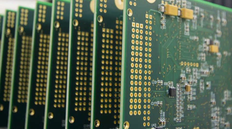
Now, let’s go through the specialized manufacturing processes involved in fabricating HDI printed circuit boards.
1. Inner Layer Formation
HDI PCBs typically begin with a multilayer board core consisting of alternating conductive copper and insulating dielectric buildup layers that are bonded together.
The core layers are fabricated separately using standard multilayer PCB processes like:
- Imaging/etching conductive layers
- Laying up dielectric prepreg/cores
- Drilling through vias
- Plating copper in drilled holes
- Laminating layers under heat and pressure
- Planarizing outer layers
However, the layer count is usually higher and layer thickness lower compared to conventional multilayer boards. The inner layers serve as the starting point for outer layer HDI buildup.
2. Surface Preparation
Once the PCB core is complete, the outer layer goes through a careful preparation process:
- Cleaning – The oxidized copper surfaces are cleaned to remove contamination. Plasma or chemical cleaning processes are typically used.
- Surface Treatment – A chemical surface treatment is applied to micro-roughen the copper surface and promote adhesion of the dielectric buildup layers.
Proper cleaning and surface treatment ensures good adhesion and prevents delamination during subsequent processing.
3. Photoresist Application
Photoresist films are laminated onto the prepared copper surfaces. These light-sensitive polymers will later be patterned into the dielectric buildup layers surrounding the traces.
4. Laser Direct Imaging (LDI)
LDI machines use a laser to precisely image the circuit pattern onto the photoresist layers. A laser beam traces out the desired circuit traces, chemically altering the resist.
This direct imaging eliminates mask imaging and alignment issues associated with standard lithographic processes. The laser can image extremely fine features down to 15μm or below.
LDI enables the very dense trace/space patterning required in HDI PCBs.
5. Photoresist Development
After LDI, the boards pass through a chemical developer. This removes the resist that was exposed to the laser, while the unexposed resist remains.
This leaves a pattern of photoresist corresponding to the desired dielectric buildup layers surrounding the circuit traces.
6. Copper Electroplating
The boards are electroplated with new copper to build up the conductive traces and interconnections within the photoresist mold.
Plating thickness is precisely controlled to achieve target trace heights and ensure uniformity across the board.
7. Photoresist Stripping
Once plating is complete, the remaining photoresist is chemically stripped away. This reveals the built up copper circuitry surrounded by dielectric.
8. Microvia Formation
Microvias are selectively formed to interconnect the conductor layers. This is a critical process for HDI boards.
Small holes are selectively ablated through the dielectric using laser drilling or plasma etch techniques. Vias down to 75-125μm diameter can be reliably formed.
The microvias are then plated with copper to form electrical connections between layers.
9. Sequential Buildup
Steps 3-8 are then repeated sequentially to build up additional alternating conductive and dielectric layers:
- Layup, image, and develop more dielectric photoresist
- Electroplate new copper traces
- Strip resist and form additional microvias
- Repeat process to build complete interconnect structure
This sequential process allows construction of a complex, high-density multilayer board. The designer has flexibility to tailor the layer stackup.
10. Outer Imaging/Etching
Final photoresist patterning and copper etching of the outmost layers completes the fine patterning of traces and pads. This defines the solderable component interconnections.
11. Solder Masking
A protective solder mask layer is applied over the entire board surface, except areas needing soldering (pads, lands, etc). This prevents solder bridging between traces.
Openings in the mask are patterned with LDI or photoimaging processes.
12. Surface Finish
An appropriate surface plating like immersion gold, ENIG, or OSP is applied to protect exposed copper and provide good solderability.
This completes the HDI PCB fabrication process. The finished boards can then be tested, inspected, and prepared for assembly.
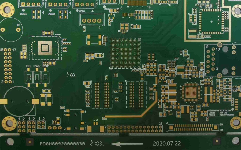
HDI PCB Testing and Quality Control
Throughout the fabrication process, rigorous testing and inspection ensures quality:
- Automated optical inspection (AOI) checks for defects.
- Electrical testing verifies continuity and connections.
- Microsectioning confirms proper layer alignment and integrity.
- Surface roughness tests ensure proper adhesion.
- Dimensions on lines/spaces, hole sizes, etc. are measured under microscopes.
- High magnification inspection identifies micro defects.
With stacked tolerances from the dense features in HDI boards, highly controlled processes paired with comprehensive testing is essential to prevent yield and quality issues.
HDI PCB Applications
The small, high-density characteristics of HDI PCBs make them well suited for many advanced electronics:
Consumer Electronics
- Smartphones
- Tablets/laptops
- Wearables
- Digital cameras
Automotive Electronics
- Engine control units
- Infotainment systems
- ADAS modules
Medical Electronics
- Implants
- Wearable monitors
- Portable instruments
Aerospace/Defense
- Avionics
- Radars
- Communications
Computing
- Servers
- Routers/network gear
- Data storage devices
And more. Any application with size constraints, performance requirements, or high interconnect densities can benefit from HDI PCB technology.
Comparison to Standard PCB Manufacturing
HDI PCB fabrication has some notable differences from conventional PCB manufacturing processes:
| HDI PCBs | Standard PCBs |
|---|---|
| Laser direct imaging of traces | Standard lithography with masks |
| Sequential buildup process | Simultaneous lamination |
| Thinner dielectric layers | Thicker laminated cores |
| Blind and buried microvias | Through-hole vias |
| Fine lines/spaces (<25um) | Larger features (>50um) |
| Microvia diameters <150um | Larger mechanically drilled vias |
| Typical layer count >6 | Typically only 4-8 layers |
The combination of these advanced fabrication techniques enables HDI PCBs to achieve the densities and performance needed for many modern electronics applications.
Benefits and Challenges of HDI PCBs
Benefits
- Increased circuit density and component packing
- Miniaturization of products
- Improved electrical performance from tighter traces
- Higher interconnect density from microvias
- Enables advanced, multi-layer designs
- Allows embedding of components
- Reduces layers needed for complex designs
Challenges
- Fabrication is more complex and costly
- Tighter process controls required
- Testing/inspection for micro-defects
- Thermal management concerns from densification
- Often limited to advanced PCB shops
- Design complexity from dense layouts
Conclusion
HDI PCB manufacturing integrates a series of advanced fabrication processes such as laser direct imaging, sequential buildup, and microvias to enable the ultra-fine features and high densities required in many modern electronics.
However, with stacked dimensional tolerances, high reliability requirements, and little room for error, fabricating HDI boards necessitates strict process controls and comprehensive testing/inspection at each process step.
While more complex and costly than conventional PCBs, the benefits of miniaturization, increased functionality, improved electrical performance, and enabling of advanced electronics make HDI PCB technology an important option for engineers and designers.
Frequently Asked Questions
Here are some common FAQs about HDI PCB manufacturing:
Q: What are the key characteristics of HDI PCBs?
A: Fine lines/spaces (<25um), microvias (<150um diameter), thin dielectrics (25-50um), high layer count (>6), and high interconnect density (>20 pads/mm2). This enables increased circuit densification vs. standard PCBs.
Q: What are the most critical processes for HDI PCBs?
A: Laser direct imaging for fine patterning capability, microvia formation to interconnect layers, and the sequential buildup process to construct multilayers.
Q: What are some typical applications of HDI PCB technology?
A: Consumer electronics like smartphones and tablets, automotive electronics, medical devices, aerospace/defense products, computing devices, and other space-constrained or high performance applications.
Q: What are some key design considerations for HDI PCBs?
A: Accounting for fine feature fabrication tolerances, minimizing unnecessary vias, planning for thin dielectrics, utilizing blind/buried vias, allowing adequate annular rings on microvias, and working closely with your PCB manufacturer on design for manufacturability guidelines.
Q: How does reliability of HDI PCBs compare to standard PCBs?
A: With proper design and fabrication, HDI PCB reliability can match or exceed standard PCBs. However, the smaller features are less tolerant of defects, requiring tighter process controls and testing to ensure quality and prevent field failures.


Leave a Reply