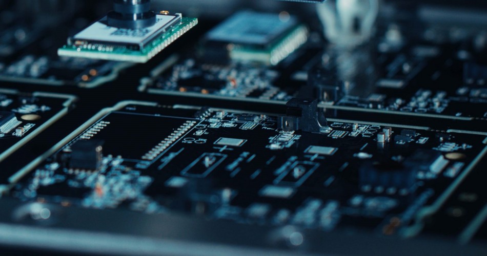
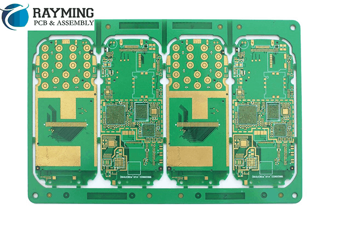
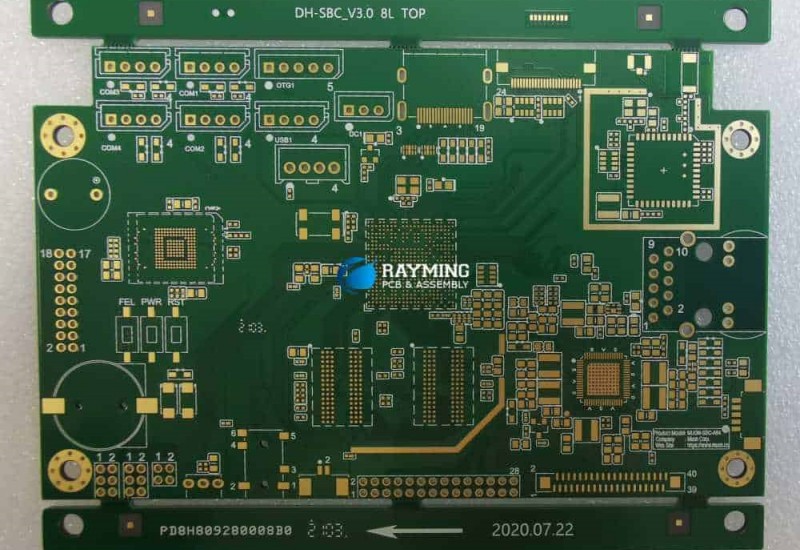
Introduction to HDI PCBs
HDI (High Density Interconnect) PCBs refer to printed circuit boards with a higher wiring density than traditional PCBs. They allow trace spacings and wire widths under 100 microns, whereas standard PCBs only allow minimum spacings of around 150 – 250 microns.
HDI PCBs provide the following benefits:
- Smaller overall size – More room for components and features in a compact design
- Higher component density – Fit more components in the same area
- Shorter routing distances – Faster signal transfer speeds
- Less noise and crosstalk – From tighter trace spacing and thinner dielectric materials
- Layer count reduction – By moving to finer trace widths and spacing
Some key technologies used in HDI PCBs include:
- Microvias – Small vias with diameters under 150 microns
- Thin core dielectric materials – Thinner insulating substrate layers
- Laser drilling – To reliably produce microvias
- Fine line circuitry – Lines and spaces under 100 microns
- Thin copper – As thin as 1 oz copper to allow fine traces
Industries Using HDI Technology
HDI PCBs are widely used in miniaturized and high performance products across many industries:
Consumer Electronics
Smartphones, tablets, wearables, and other consumer gadgets all utilize HDI PCBs to fit more functionality into compact form factors. The tight spacing enables more processor power, memory, sensors, and wireless connectivity.
Automotive Electronics
In-vehicle infotainment, advanced driver assistance systems, and electric powertrains rely on HDI PCBs. The boards integrate many components including applications processors, GPUs, memories, power management ICs, and connectors.
Medical Devices
Hearing aids, blood glucose monitors, and diagnostic imaging tools need advanced PCBs. HDI allows more capabilities like wireless connectivity to be packed into tiny medical devices.
Aerospace and Defense
Avionics, radars, and other military systems use HDI PCBs. Size and weight reduction is critical in aerospace applications. The boards also withstand shock, vibration, and extreme temperatures.
Manufacturing Capabilities Needed
Producing HDI PCBs requires advanced manufacturing capabilities:
- Fine line circuitry – Lines/spaces under 100μm need precise imaging and etching equipment. Laser direct imaging (LDI) is commonly used.
- Tight alignment – Aligning layers with microvia interconnects requires highly accurate registration systems. Automated optical inspection (AOI) ensures quality.
- Thin materials – Special prepregs, cores, and copper foils are needed. Careful handling minimizes warp and wrinkles.
- Microvias – Laser drilling machines reliably produce small diameter vias. Depth control and tapering are critical.
- Sequential lamination – Building up HDI layers often uses a specialized process to embed microvias. Tight process controls prevent reliability issues.
- Finishing – Plating, coating, solder mask, and legend printing must work with fine features. Cleanliness is imperative.
- Inspection – High magnification inspection cameras and x-rays catch defects. Testing verifies electrical connectivity and performance.
Design Considerations for HDI
HDI PCB design requires close coordination between designers and fabrication partners:
- Stackup – Selecting dielectric materials and layer count based on electrical, thermal, and mechanical needs.
- Routing – Optimizing trace routing to take advantage of HDI capabilities for density and speed.
- Components – Choosing the right high density components suited for fine pitch soldering.
- Thermal – Incorporating adequate thermal management for high power components and chips.
- Test – Designing test points, fixtures, and access around dense HDI circuitry.
- Simulation – Modeling and verifying signal and power integrity early in the design flow.
- DFM – Following design for manufacturing guidelines tailored to your vendor’s HDI process.
- Data handoff – Comprehensive Gerber and netlist data formatted for your vendor’s CAM and inspection needs.
Careful HDI design results in maximum utilization of the board’s capabilities while ensuring manufacturability.
HDI PCB Applications
Here are some specific product examples highlighting how HDI PCB technology enables advanced functionality:
Smartphones
HDI is used extensively in smartphones for the main logic board, memory modules, and other sub-boards. Apple’s iPhone 14 Pro has a 6 layer HDI board packed with an A16 processor, 5G modem, and other chips. The compact size rivals laptop computing power.
Wearable Health Trackers
Fitness bands and smartwatches integrate health monitoring sensors, battery, antenna, and processor into a tiny wrist-worn package. For example, the Samsung Galaxy Watch 5 Pro uses HDI flex boards to connect the compact chip packages to the curved display.
Hearing Aids
Next generation hearing aids add wireless audio streaming and voice capabilities. Starkey’s Livio AI hearing aid has an 8 layer HDI PCB with microvias supporting far-field microphones, rechargeable batteries, audio DSP, and Bluetooth connectivity.
Satellite Communications
Satellites for broadband internet like SpaceX’s Starlink pack phased array antennas and high power transmitters into small modules. HDI allows routing for thousands of tiny antenna elements while handling significant power levels.
Military Radars
Advanced air and missile defense radar systems require digital beamforming. HDI PCBs in each radar module connect hundreds or thousands of individually controlled transceiver elements for electronic beam scanning and shaping.
Drone/UAV Autopilots
Miniature inertial measurement units and flight controllers guide autonomous drones. Pixhawk autopilot modules designed for drones like the DJI Mavic contain multiple HDI PCBs to integrate MEMS sensors, processors, and power management.
Conclusion
HDI PCB technology enables miniaturization and performance advances in many of today’s electronic devices. As components continue shrinking and circuit speeds increase, HDI will become a mainstream PCB technology. Close coordination between designers and manufacturers is key to realizing the benefits.
Frequently Asked Questions
What are some key differences between HDI and conventional PCBs?
The main differences are smaller trace widths and spaces (below 100 microns vs. 150+ microns), smaller microvias (below 150 microns vs. 250+ microns), and thinner dielectric materials in the HDI stackup. This allows higher wiring density and component density.
What are the main reliability risks to watch out for with HDI PCBs?
Some risks include: microvia cracks and opens from thermal stress or drilling issues, fine line cracks from handling or vibration, thinner dielectrics increase electrical shorts risk, and contamination causing electrochemical migration along tight lines.
How many HDI layers are typically used?
Most designs use between 4-8 layers, but some complex designs go up to 10 layers or more. High layer counts increase manufacturing complexity and cost.
What design tools are typically used for HDI PCBs?
Specialized PCB layout tools like Mentor Xpedition, Cadence Allegro, and Altium Designer have extensive HDI design rule checks, constraint managers, and modeling features to facilitate robust HDI designs.
Does HDI allow smaller solder pads and finer component pin pitches?
Yes, the solder pad and trace routing can scale down to match finer component pin pitches, allowing denser component mounting. This requires accurate solder mask alignment and well-controlled solder paste printing.


Leave a Reply