
Introduction
As electronic devices become increasingly smaller and more complex, the printed circuit boards (PCBs) inside them must become denser and allow for finer features. This is where high-density interconnect (HDI) PCB fabrication comes in. HDI PCBs have finer lines and spaces, smaller vias, and more layers than conventional PCBs. This allows them to accommodate more components in less space while maintaining high performance.
In this guide, we will cover everything you need to know about HDI PCB fabrication including:
- What is HDI technology?
- Benefits of HDI PCBs
- HDI design and layout considerations
- HDI manufacturing process
- HDI testing and inspection
- HDI applications
- Costs
- FAQs
Understanding the capabilities and limitations of HDI technology will allow you to determine if it is suitable for your project. Let’s get started.
What is HDI Technology?
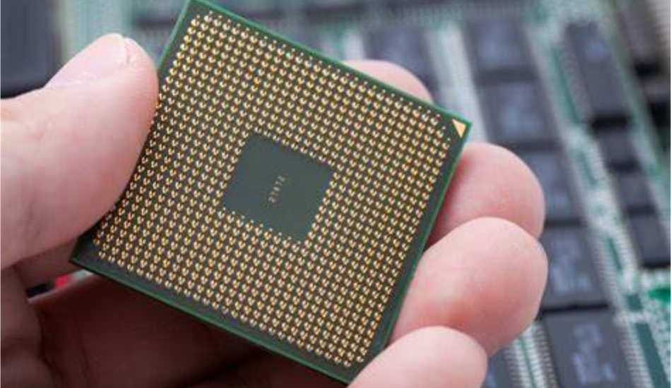
HDI stands for high-density interconnect or high-density interconnection. HDI PCBs use finer traces, spaces, and vias to increase the interconnect density compared to conventional PCBs.
Specifically, HDI PCBs have:
- Traces and spaces of 6 mils or less
- Microvias with diameters of 6 mils or less
- Stacked microvias for even greater connection density
- More layers – typically 6 to 20
To accommodate the fine features, HDI PCBs also require dielectric materials with extremely low loss such as polyimide. This helps maintain signal integrity at high frequencies.
The IPC-2226 standard defines three classes of HDI technology:
HDI Classes
| Class | Lines/Spaces | Microvia Diameter |
|---|---|---|
| HDI Class I | ≤ 4/4 mils | ≤ 4 mils |
| HDI Class II | ≤ 3/3 mils | ≤ 4 mils |
| HDI Class III | ≤ 2/2 mils | ≤ 4 mils |
So in summary, HDI PCB technology uses finer traces and microvias to increase interconnect density beyond what is possible with conventional PCB fabrication processes. This allows for miniaturization and improved electrical performance.
Benefits of HDI PCBs
Let’s look at some of the key benefits that HDI PCB technology provides:
Higher Interconnect Density
The main advantage of HDI PCBs is the increased interconnect density. More connections can fit in the same area. This enables miniaturization and thinner overall package sizes.
Layer Count Reduction
Because routing space is used more efficiently, HDI PCBs can achieve the same functionality with fewer layers. A 6-8 layer HDI PCB can replace a 12-16 layer conventional PCB. Fewer layers reduces cost and thickness.
Improved Electrical Performance
With narrower traces and spaces, HDI PCBs can minimize noise coupling and crosstalk. Microvias provide low inductance connections between layers. This results in improved signal integrity at high frequencies.
Reduced Power Consumption
The finer features mean lower capacitance which reduces power consumption. Thinner PCBs also require less power.
Enhanced Reliability
Microvias and thin dielectrics provide a high strength interconnect with low stress and resistance to thermal cycling and vibration. This improves reliability and product lifetime.
Design Flexibility
HDI technology provides more routing channels and flexibility to route high density connections on the PCB. This facilitates complex or high pin count IC designs.
In summary, HDI PCB fabrication enables smaller, higher performing, and more reliable products across a wide range of applications from smartphones to aerospace systems.
HDI Design and Layout Considerations
Designing a PCB using HDI technology requires some unique considerations:
Dielectric Materials
The dielectric layers must have a low loss tangent, high glass transition temperature, and low coefficient of thermal expansion to maintain signal integrity and reliability with the increased circuit density. Some common HDI dielectrics are polyimide, BT resin, PPE, and liquid crystal polymer.
Trace Width and Spacing
Follow the fabricator’s design rules for minimum trace width and spacing. For impedance matching, use their guidelines for calculating trace widths based on stackup, layer thickness, and dielectric constant.
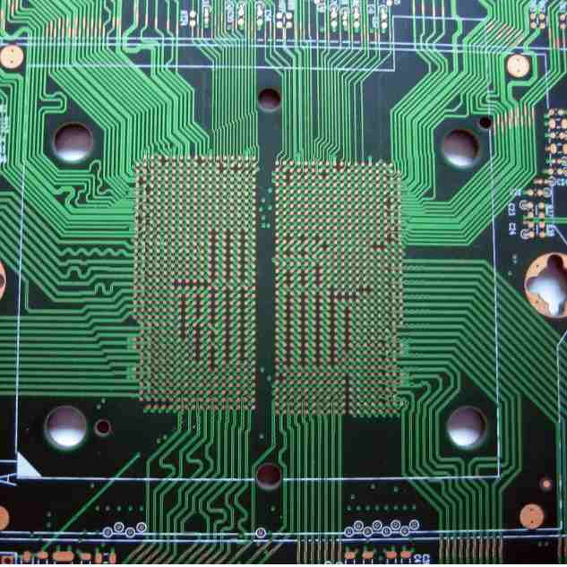
Microvias
Minimize connection distance when routing to microvias. Follow the aspect ratio limits for microvia depth vs diameter to ensure reliability. Recommended ratios are 1:1 to 4:1 max.
Stacked Microvias
Use stacked microvias when more than one connection is needed between layers. Offset the vias slightly when stacking to improve etchability and prevent voids.
Capture Pads
Use capture pads for connecting traces to microvias. This provides greater alignment tolerance and improves reliability. Recommended capture pads are 4-5 mils larger than the drill diameter.
Plane Layers
Include uninterrupted power and ground plane layers whenever possible. This enhances signal integrity at high frequencies. Use numerous narrow cutouts rather than large cutouts in planes.
Layer Transition Vias
When transitioning between HDI and conventional layer segments, place vias strategically to avoid stub traces, excessive bends, and impedance discontinuities.
Proper HDI design practices, close collaboration with your PCB fabricator, and following their capabilities and design rules will ensure a successful project.
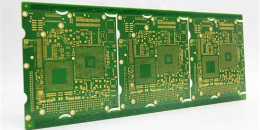
HDI Manufacturing Process
Fabricating HDI PCBs requires specialized processes to produce the fine features and high interconnect density. Here is an overview of the HDI manufacturing process flow:
Layer Preparation
The individual dielectric and foil core layers are prepared first. Dielectrics like polyimide are laminated with copper foil. Alignment holes are drilled or punched.
Imaging
A photoresist coating is applied and then imaged using advanced photolithography techniques to produce traces and spaces of 6 mils or below.
Etching
The copper is etched to form the desired circuit pattern held in the photoresist. Precision etching is critical for fine features.
Microvia Drilling
Microvias are drilled using laser drilling. Mechanical drilling can also be used but laser offers superior accuracy for small vias. The holes are 6 mils or less in diameter.
Plating
An electroless copper plating is applied first to coat the hole walls. Then electrolytic copper plating to fill the microvias and build up trace thickness.
Outer Layer Lamination
Individual core layers are aligned using the pre-drilled holes then laminated together under heat and pressure to form a multi-layer board.
Via Protection
Dry film or liquid photoimageable resist (LPI) is applied and imaged to form a protective layer over the microvias. This prevents damage during outer layer processing.
Outer Layer Imaging and Etching
The outer layer circuitry pattern is formed using photolithography and copper etching as done previously for the inner layers.
Solder Mask and Silkscreen
Solder mask and legend are printed using liquid photoimageable ink to define solderable areas and printidentification.
Surface Finishes
OSP, ENIG, or other metallic finishing is applied to protect exposed copper traces from oxidation and improve solderability.
Electrical Test
Each completed PCB is electrically tested for opens, shorts, and functionality using specialized flying probe or fixture testers.
This provides a high-level overview of the additional steps and precision required to produce HDI PCBs compared to conventional PCB fabrication. Tight process controls and automation helps achieve the fine features and align layers accurately.
HDI Testing and Inspection
Verification testing is critical with HDI PCBs given the tight tolerances involved. Here are some of the testing methods used:
- Automated Optical Inspection (AOI): Used after imaging, etching, drilling, and solder mask steps. Detects defects like opens, shorts, nicks, spots, etc.
- Laser Via Inspection: Laser scanning to validate microvia quality – taper, barreling, roundness, etc. Done after drilling.
- Impedance Testing: Tests electrical impedance of traces to ensure match to design specifications. Uses specialized coupons.
- High magnification inspection: 100x to 200x magnification inspection of line features and text print quality.
- X-Ray Inspection: X-ray images used to inspect buried vias and features for defects. Checks for proper fill plating.
- Cross-Sectioning: Cutting cross-section samples to inspect plating quality and layer alignment under microscope.
- Flying Probe Testing: Electrical test of nets, traces, and test points. Detects opens, shorts, and functionality fails.
- ICT and Functional Test: Tests board interconnectivity, continuity, and functional performance.
HDI PCB suppliers will utilize a combination of these inspection and test methods to fully verify and qualify the fabrication process is meeting requirements.
HDI Applications
Some of the key application areas that benefit from HDI PCB technology include:
Smartphones
HDI allows smartphone PCBs to achieve the component density required while minimizing thickness. The enhanced electrical performance also helps maintain signal integrity at cellular data rates.
Wearable Electronics
Miniaturization is critical for wearable devices. HDI provides the interconnect density necessary in a much smaller footprint.
Internet of Things (IoT)
Many networked sensors and devices need complex PCBs to fit into very compact enclosures. HDI enables greater functionality per unit area.
High Speed Networking
Switches, routers, servers and other networking equipment operate at multi-Gigabit data rates. HDI maintains signal quality and integrity across backplanes and cards.
Automotive Electronics
The number of electronic control modules in vehicles is rapidly increasing. HDI allows for reducing size and weight of these modules.
Aerospace and Defense
Military systems require reliability along with miniaturization. HDI offers this through dense, robust interconnects on deployable electronics.
HDI technology is becoming a requirement for many advanced electronics products to meet size, performance, and reliability needs.
HDI Fabrication Cost Considerations
As with any advanced PCB technology, HDI comes with increased costs compared to standard PCB fabrication. Here are some of the key drivers:
- Material Costs: The base dielectric and foil materials required for HDI are more expensive. Polyimide and metal foil cores add cost.
- Additional Processing: HDI boards require more fabrication steps like microvia drilling/filling and advanced imaging techniques.
- Low Yields: The tight tolerances yield more scrapped boards during fabrication until the process is optimized. This adds cost.
- Advanced Testing: Extensive inspection and electrical testing is needed to validate HDI boards which adds cost.
- Small Quantities: Prototyping or low volume HDI runs don’t benefit from economies of scale which keeps costs higher.
- Design Complexity: Intricate HDI boards with maximum density take more engineering time which adds cost. Simpler designs save on engineering.
Like most advanced technologies, HDI costs have decreased over time as manufacturing methods have improved. Work closely with your fabricator to maximize cost savings through design optimization and larger order quantities when possible.
FAQs
Here are some frequently asked questions about HDI PCB fabrication:
Q: At what layer count does it make sense to use HDI technology?
A: Typically 6 layers is a good starting point to consider HDI instead of conventional PCBs. The layer reduction and density benefits of HDI start to provide advantages at 6 layers or more.
Q: Can microvias replace through hole vias?
A: Not entirely. Microvias are best for connecting adjacent layers. Some through hole vias are still needed to connect the outermost layers or provide mechanical anchoring. The number of through holes can be minimized though.
Q: What are the limitations of HDI trace widths and microvia sizes?
A: The current limitations are trace/space of 2/2 mils and microvia diameters of 2 mils. As fabrication methods advance, some vendors can achieve 1/1 mil features. But this is still emerging capability.
Q: Can multiple microvia diameters be combined on one HDI PCB?
A: Yes, as long as the fabrication process can support the smallest microvia size, mixed microvia dimensions can provide flexibility for higher density in certain areas and lower density where less interconnect is required.
Q: Are there any reliability risks with HDI PCBs?
A: With proper design and fabrication methods, HDI boards can actually demonstrate better reliability than conventional boards. The lamination process helps compensate for greater CTE and modulus mismatches. And short connections reduce susceptibility to thermal cycling and vibration stresses.
Conclusion
HDI technology enables the level of miniaturization, component density, and electrical performance required in many of today’s cutting edge electronic products. As PCBs become more compact with greater functionality integrated, HDI fabrication provides a solution where conventional PCB technology falls short.
Collaborating early with your PCB manufacturer to incorporate HDI design practices tailored to their capabilities is key to a successful implementation. The investment in HDI will pay dividends through enhanced product functionality and reliability along with potential size and weight reduction.
So in summary, consider utilizing HDI printed circuit boards when you need:
- Fine features for increased circuit density
- High component counts in small areas
- High frequency electrical performance
- Reduced layer counts
- Improved power efficiency
- Robust interconnect reliability
- Lighter weight and thinner profiles
By understanding where and how to take advantage of HDI technology for your next product, you can fully leverage the benefits this advanced PCB fabrication process provides.


Leave a Reply